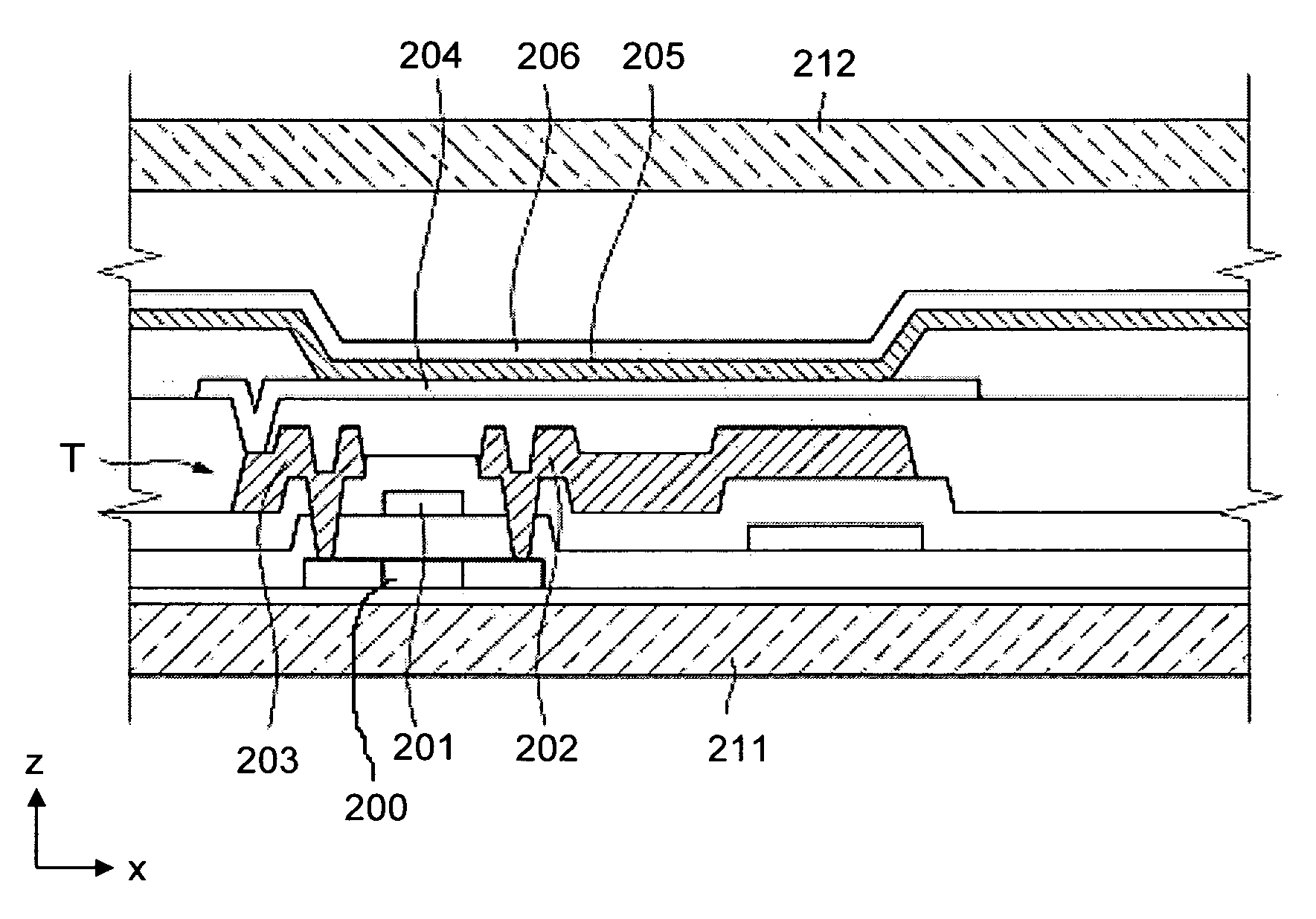
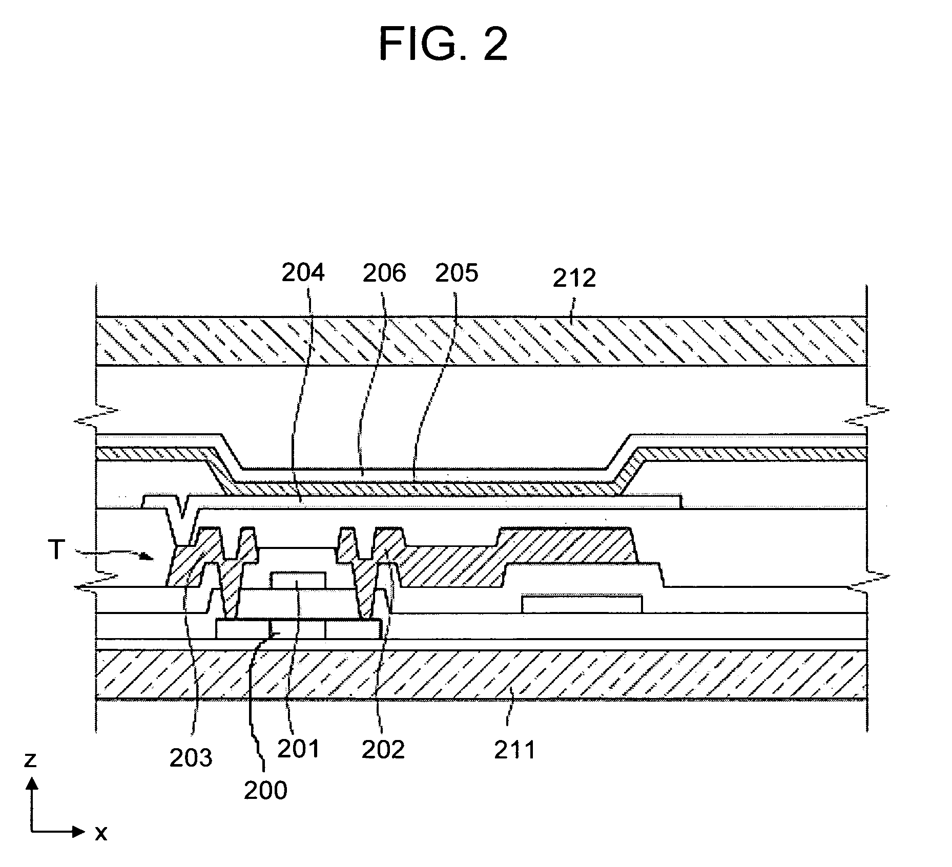
Organic light emitting diode and method of fabricating the same
a light-emitting diode and organic technology, applied in the direction of thermoelectric device junction materials, electrical equipment, semiconductor devices, etc., can solve the problems of poor picture quality of the light-emitting diode, small amount of light from the light-emitting diode, etc., to reduce the efficiency of electron injection, low brightness, and low luminous efficiency
- Summary
- Abstract
- Description
- Claims
- Application Information
AI Technical Summary
Benefits of technology
Problems solved by technology
Method used
Image

Examples
experimental example 1
[0040]A first electrode was formed of indium tin oxide (ITO) to a thickness of 130 nm. Subsequently, a hole injection layer, which was made of IDE-406 (manufactured by Idemitsu) as tertiary amine compound to a thickness of 210 nm, was formed on the first electrode, and a hole transport layer, which was made of NPB to a thickness of 20 nm, was formed on the hole injection layer. A red phosphorescent emission layer having a thickness of 40 nm was formed on the hole transport layer using a mixture of CBP as a host and Ir(piq)3 as a dopant at a concentration of 15 wt %. An electron transport layer, which was made of Alq3 to a thickness of 30 nm, was formed on the red phosphorescent emission layer. Subsequently, a metal layer, which was made of Mg as a single metal element to a thickness of 10 Å, was formed on the electron transport layer. A second electrode, which was formed of an MgAg layer to a thickness of 200 Å, was formed on the metal layer.
experimental example 2
[0041]An organic light emitting diode was prepared in the same manner as in Experimental Example 1, except that a metal layer was made of Mg as a single metal element to a thickness of 30 Å.
PUM
 Abstract
Description
Claims
Application Information
 - R&D Engineer
- R&D Manager
- IP Professional
- Industry Leading Data Capabilities
- Powerful AI technology
- Patent DNA Extraction
Browse by: Latest US Patents, China's latest patents, Technical Efficacy Thesaurus, Application Domain, Technology Topic.
© 2024 PatSnap. All rights reserved.Legal|Privacy policy|Modern Slavery Act Transparency Statement|Sitemap