
Correction of parasitic capacitance effect in touch sensor panels

a capacitance effect and capacitance correction technology, applied in the field of multitouch sensor panels, can solve problems such as false detection of negative touch, and achieve the effect of improving accuracy and facilitating calculation of object-to-ground capacitan

Active Publication Date: 2010-03-11
APPLE INC
View PDF31 Cites 179 Cited by
  • Summary
  • Abstract
  • Description
  • Claims
  • Application Information

AI Technical Summary

Benefits of technology

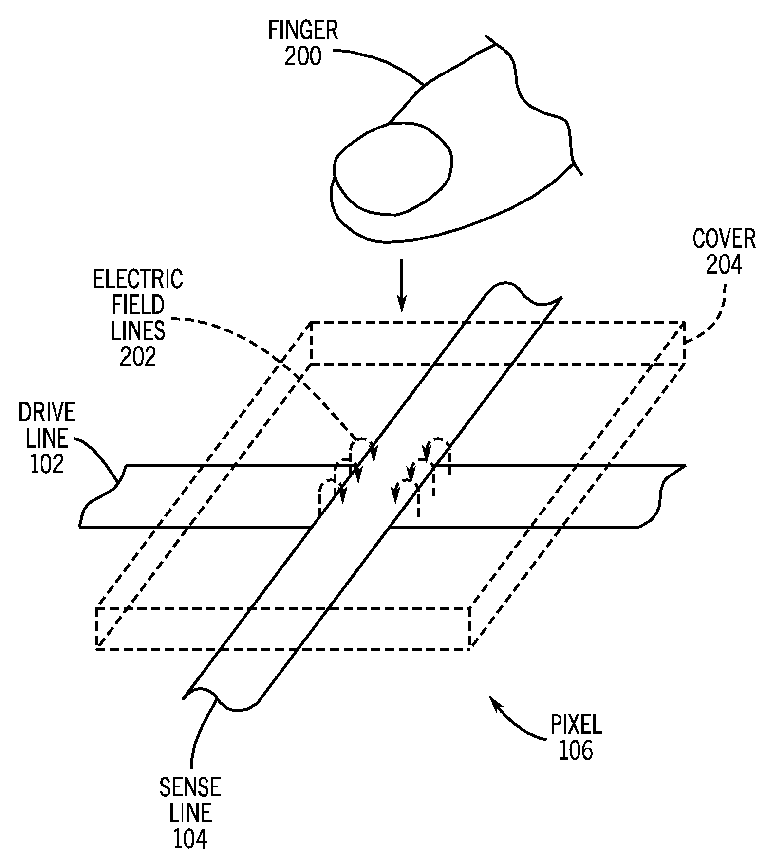
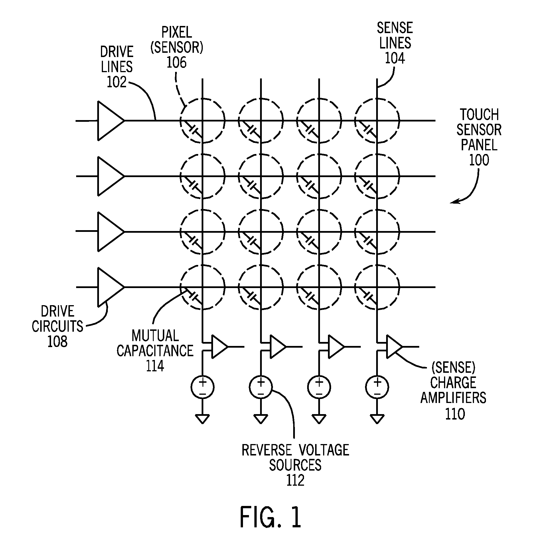
[0006]Erroneous detection of what appears to be negative touch event(s) may occur when a user is touching one or more locations on the touch sensor panel but fails to also be in good contact with another part of the device including the touch sensor panel. To compensate for these erroneous readings, sense lines of the touch sensor panel can include reverse driving circuits to facilitate calculation of an object-to-ground capacitance. This capacitance is periodically calculated during normal operation of the touch sensor panel to identify when the touch sensor panel is being touched under poor grounding conditions. If the calculated object-to-ground capacitance indicates the presence of a poor grounding condition, then the object-to-ground capacitance and detected pixel touch output values are used to estimate new pixel touch output values in an iterative manner. These new values represent estimates of the actual pixel touch output values and are used in place of the detected pixel touch output values to actually determine touch event(s). Accordingly, improved accuracy is provided for determining touch event(s) on a touch sensor panel.

Problems solved by technology

Erroneous detection of what appears to be negative touch event(s) may occur when a user is touching one or more locations on the touch sensor panel but fails to also be in good contact with another part of the device including the touch sensor panel.

Method used


Image

  • Correction of parasitic capacitance effect in touch sensor panels
  • Correction of parasitic capacitance effect in touch sensor panels
  • Correction of parasitic capacitance effect in touch sensor panels

Examples


Embodiment Construction

[0023]In the following description of preferred embodiments, reference is made to the accompanying drawings which form a part hereof, and in which it is shown by way of illustration specific embodiments in which the invention can be practiced. It is to be understood that other embodiments can be used and structural changes can be made without departing from the scope of the embodiments of this invention.

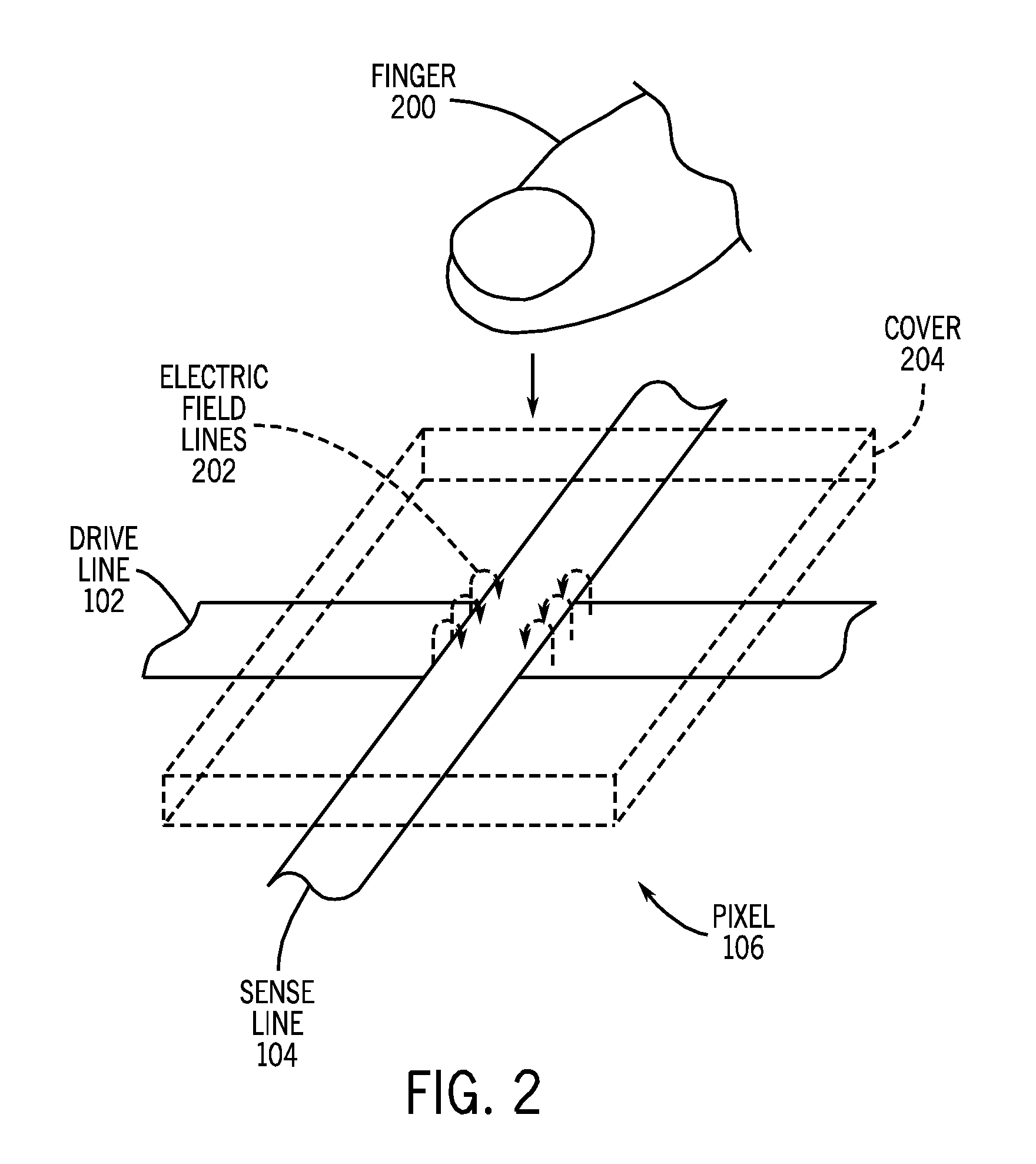
[0024]Embodiments of the invention relate to correction of erroneous detection of touch event(s) on a touch sensor panel. Erroneous detection of what appears to be negative touch event(s) (e.g., so-called “negative pixels”) may occur when a user is touching one or more locations on the touch sensor panel but fails to also be in good contact with another part of the device including the touch sensor panel. To compensate for these erroneous readings, sense lines of the touch sensor panel can include reverse driving circuits to facilitate calculation of an object-to-ground capacitance. ...


PUM


Abstract

Compensation of pixels included in a touch sensor panel that generate erroneous readings (so called “negative pixels”) due to a poor grounding condition of the object touching the touch sensor panel is disclosed herein. To compensate for the erroneous readings, sense lines of the touch sensor panel can include reverse driving circuits to facilitate calculation of an object-to-ground capacitance. If the calculated object-to-ground capacitance indicates the presence of a poor grounding condition, then the object-to-ground capacitance and detected pixel touch output values are used to estimate new pixel touch output values that are used instead of the detected pixel touch output values to determine touch event(s).

Description

FIELD OF THE INVENTION [0001]This relates generally to multi-touch sensor panels that utilize an array of capacitive sensors (pixels) to detect and localize touch events, and more particularly, to the correction of pixels having distorted readings when touch events are generated by a poorly grounded object.BACKGROUND OF THE INVENTION [0002]Many types of input devices are presently available for performing operations in a computing system, such as buttons or keys, mice, trackballs, joysticks, touch sensor panels, touch screens and the like. Touch screens, in particular, are becoming increasingly popular because of their ease and versatility of operation as well as their declining price. Touch screens can include a touch sensor panel, which can be a clear panel with a touch-sensitive surface, and a display device such as a liquid crystal display (LCD) that can be positioned partially or fully behind the panel so that the touch-sensitive surface can cover at least a portion of the view...

Claims


Application Information

Patent Timeline
IPC IPC(8): G06F3/045H04B1/38
CPCG06F3/044G06F3/0418G06F2203/04104G06F3/04186G06F3/0446G06F3/0445
Inventor YOUSEFPOR, MARDUKE
Owner APPLE INC
Learn More