System and method for detecting fluorescence in microfluidic chip

a microfluidic chip and fluorescence detection technology, applied in the field of fluorescence detection systems, can solve the problems of precise operation of the apparatus used in fluorescence detection, and achieve the effect of reducing the amount of data to be transmitted and being advantageous in communication and calculation

Active Publication Date: 2008-08-14
SAMSUNG ELECTRONICS CO LTD
View PDF7 Cites 101 Cited by
  • Summary
  • Abstract
  • Description
  • Claims
  • Application Information

AI Technical Summary

Benefits of technology

[0020]However, the present invention overcomes this problem by transmitting the detection signal of each microchamber as one data value. Then, even if the data value is 32 bit, data transmission for the eight microchambers and the six channels can be enabled by 192 bytes. Accordingly, the present invention can reduce the amount of data to be transmitted as well as is advantageous in terms of communication and calculation.

Problems solved by technology

However, there are problems in that apparatuses used in the fluorescence detection should be precisely operated to obtain correct results.

Method used


Image

  • System and method for detecting fluorescence in microfluidic chip
  • System and method for detecting fluorescence in microfluidic chip
  • System and method for detecting fluorescence in microfluidic chip

Examples


Embodiment Construction

[0030]The present invention will now be described more fully with reference to the accompanying drawings, in which preferred embodiments thereof are shown. However, it should be understood that the present invention is not limited by the embodiments.

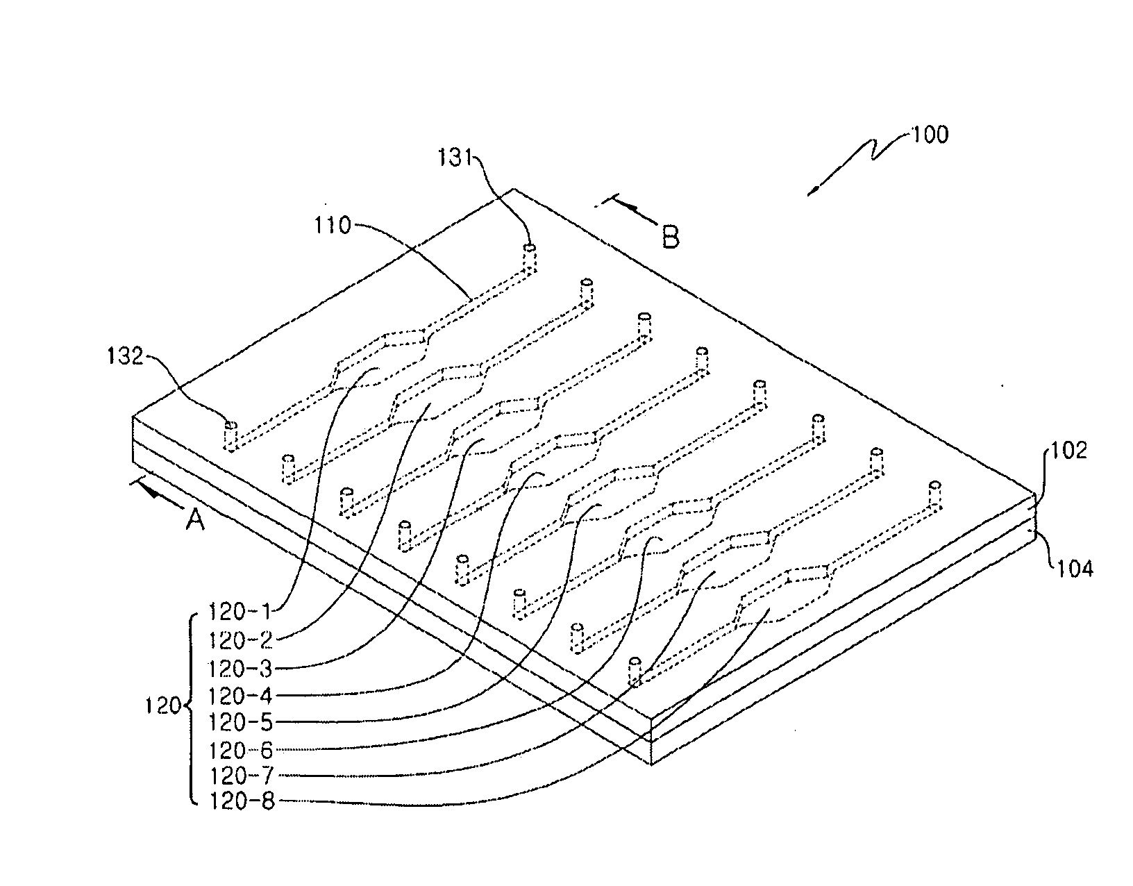
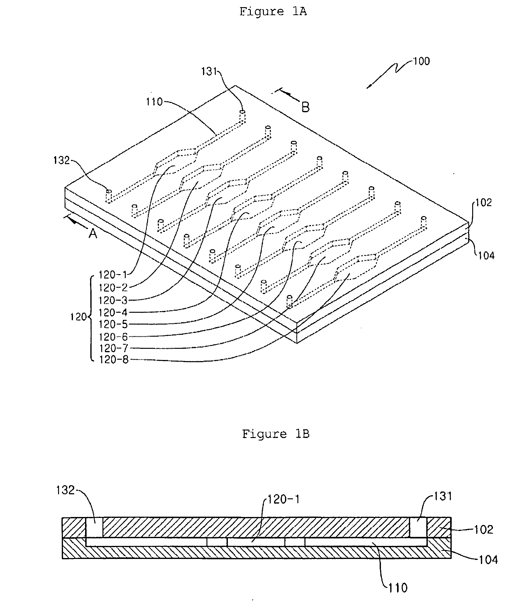
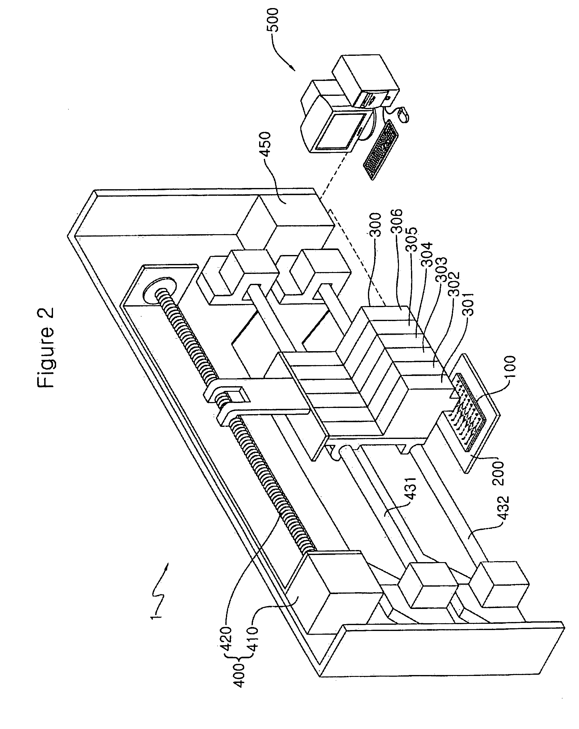
[0031]FIG. 1A is a perspective view illustrating a microfluidic chip 100 used in a fluorescence detection system according to an embodiment of the present invention, and FIG. 1B is a cross-sectional view taken along the line A-B in FIG. 1A.

[0032]The microfluidic chip 100 includes a plurality of microchambers 120, microchannels 110, inlets 131 and outlets 132. When a sample is injected into the chip 100 through the inlets 131, it enters the microchamber 120 through the microchannels 110 and remains in the microchamber 120.

[0033]The microchip 100 can be fabricated by bonding an upper substrate 102, in which the inlets 131 and the outlets 132 are engraved, to a lower substrate 104, in which the microchannels 110 and the microchambers 120 ar...


PUM

PropertyMeasurementUnit
rotation angleaaaaaaaaaa
center wavelengthaaaaaaaaaa

Abstract

A system and a method for detecting fluorescence in a microfluidic chip having a microchamber and measuring the amount of the fluorescence are disclosed. In the system and method, an optical device detects fluorescence generated by a fluorescent material. The position of the outer circumference of a microfluidic chip is identified based on the change of the amount of the detected fluorescence. Then, the position of a microchannel is calculated based on the position of the outer circumference of the microfluidic chip and the distance between the outer circumference and the microchamber. Hence, the amount of the fluorescence only generated from the microchamber of the microfluidic chip is automatically calculated. Further, a plurality of samples can be analyzed at the same time, thereby reducing analysis time and cost.

Description

CROSS-REFERENCES TO RELATED APPLICATIONS[0001]The present invention claims priority of Korean patent application number 10-2007-0012996, filed on Feb. 8, 2007, which is incorporated by reference in its entirety.BACKGROUND OF THE INVENTION[0002]1. Field of the Invention[0003]The present invention relates to a fluorescence detection system, which detects fluorescence in a microfluidic chip having a microchamber and measures the amount of the fluorescence. In addition, the present invention relates to a method for detecting fluorescence in microfluidic chip having a microchamber and measuring the amount of the fluorescence.[0004]In the fluorescence detection system of the present invention, an optical device detects fluorescence generated by a fluorescent material. The position of the outer circumference of a microfluidic chip is identified based on the amount of the detected fluorescence. Then, the position of a microchannel is calculated based on the position of the outer circumferen...

Claims


Application Information

Patent Timeline
Patent Type & Authority Applications(United States)
IPC IPC(8): G01N21/64
CPCG01N21/645G01N21/00G01N21/64
Inventor KIM, SUHYEONKIM, JINTAE
Owner SAMSUNG ELECTRONICS CO LTD
Why Eureka
Try Eureka