Substrate processing apparatus and substrate processing method

a substrate processing and substrate technology, applied in the direction of semiconductor/solid-state device testing/measurement, electric discharge tubes, decorative arts, etc., can solve the problem of large and achieve the effect of reducing the variation of incident energy of ions entering the substrate and effective reducing the voltage change of the substra

Inactive Publication Date: 2010-03-25
KK TOSHIBA +1
View PDF10 Cites 182 Cited by
  • Summary
  • Abstract
  • Description
  • Claims
  • Application Information

AI Technical Summary

Benefits of technology

[0008]It is an object of the present invention to provide a substrate processing apparatus and a substrate processing method realizing an effective reduction in a voltage change of a substrate on an electrode to reduce the variation of incident energy of ions entering the substrate.

Problems solved by technology

This causes a change in the voltage of the substrate held on the lower electrode, leading to a large variation of incident energy of the ions entering the substrate.

Method used


Image

  • Substrate processing apparatus and substrate processing method
  • Substrate processing apparatus and substrate processing method
  • Substrate processing apparatus and substrate processing method

Examples


first embodiment

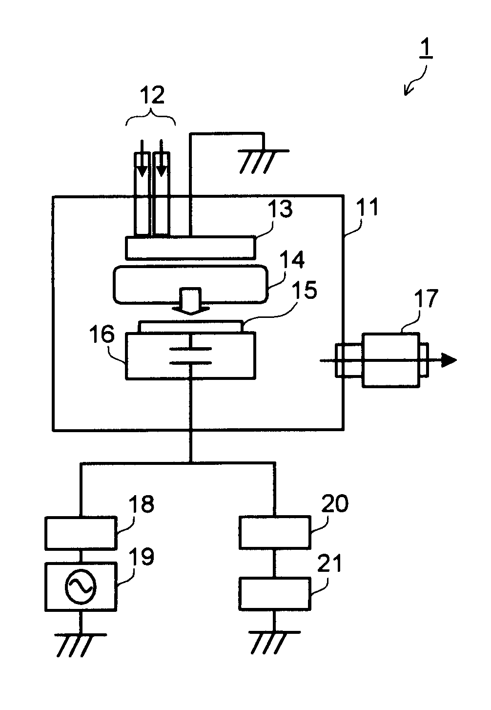
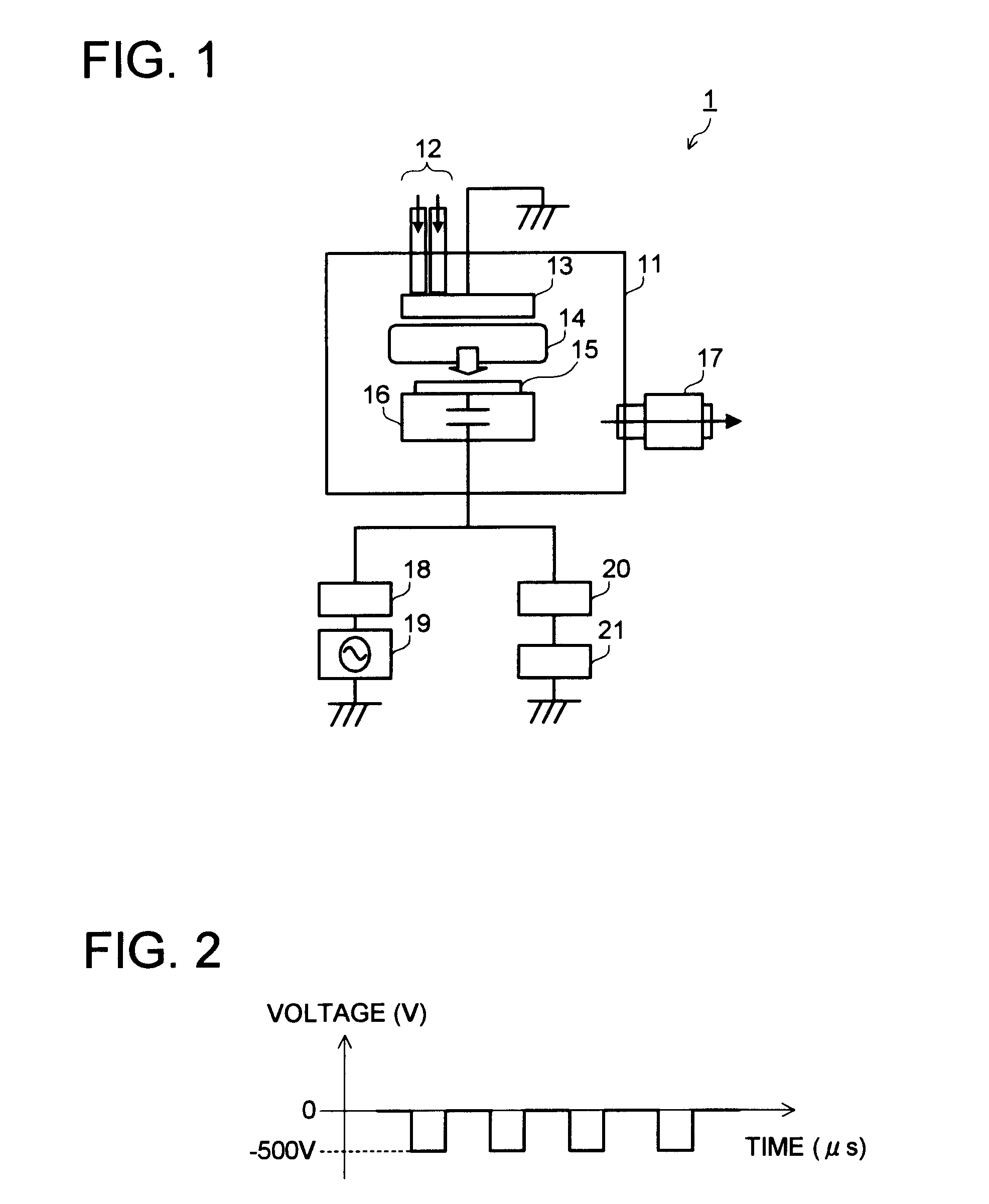
[0078]FIG. 7 is a schematic block diagram of a substrate processing apparatus 2 according to one embodiment of the present invention. FIG. 8 is a detailed block diagram of a pulse applying unit. FIG. 9 is a schematic waveform chart of a voltage applied in a superimposed manner to a lower electrode 16. In FIG. 9, the vertical axis represents voltage (Voltage) and the horizontal axis represents time (μs).

[0079]A sawtooth power source 32 outputs to a switching circuit (first switching unit) 31 a sawtooth voltage shown by a wavy line 106 in FIG. 9. Further, the sawtooth power source 32 inputs a synchronizing signal to a gate trigger 33. The synchronizing signal is input to the gate trigger 33 every arbitrary point of the sawtooth waveform shown by the wavy line 106 in FIG. 9, for example, every lowest voltage point or every highest voltage point of the sawtooth waveform.

[0080]According to the synchronizing signal input from the sawtooth power source 32, the gate trigger 33 inputs a sign...

modification examples

(Modification Examples of First Embodiment)

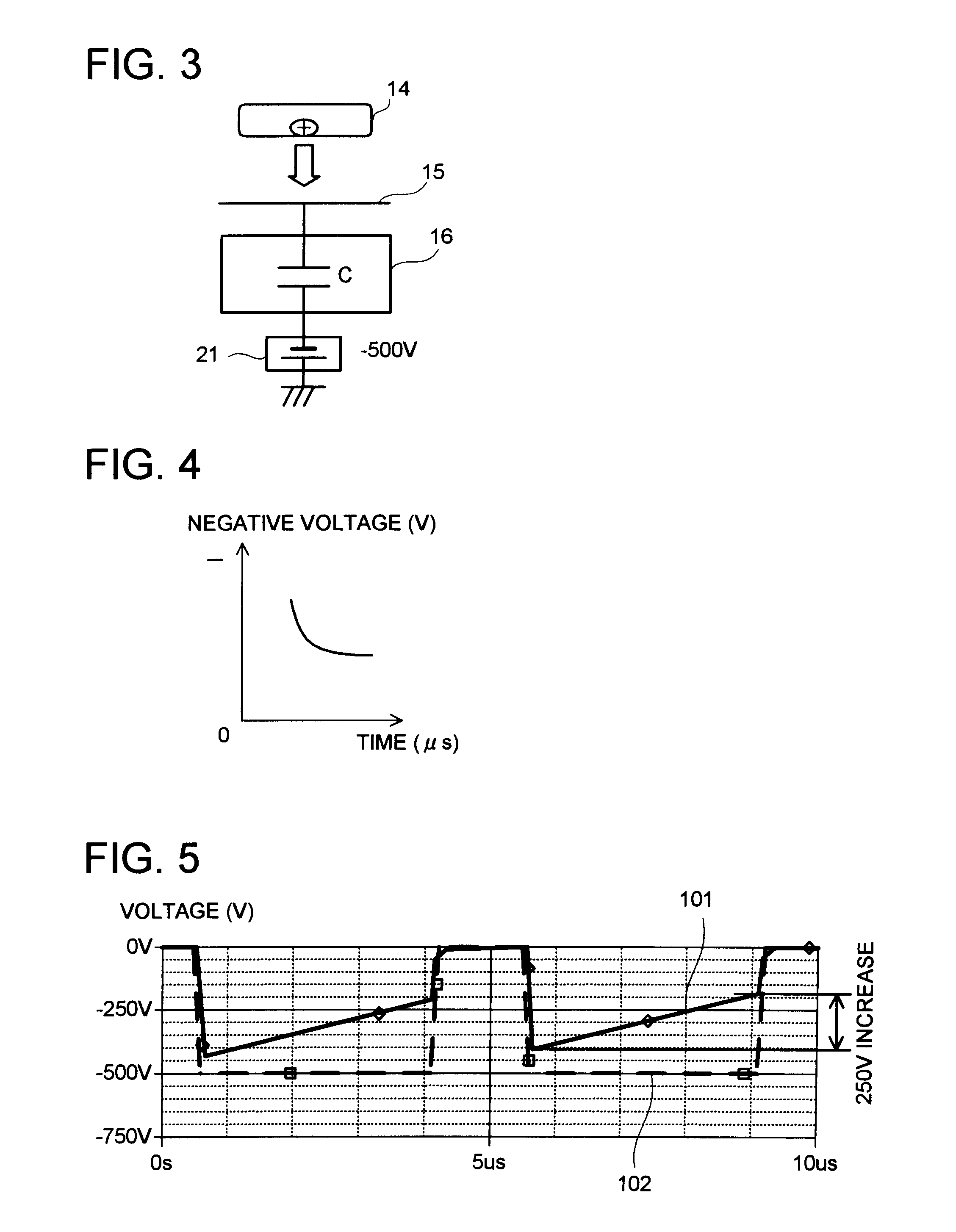
[0088]FIG. 11 and FIG. 12 are waveform charts of a voltage applied to the lower electrode 16 in modification examples of the first embodiment. In the first embodiment, the sawtooth voltage output from the sawtooth power source 32 as described with reference to FIG. 9 is taken out by the switching circuit 31, whereby the pulse voltage whose voltage in one pulse decreases in accordance with time is applied to the lower electrode 16.

[0089]However, the use of the sawtooth voltage is not necessarily essential provided that the voltage change of the wafer 15 in the course of the etching process can be reduced to 50 V or less. Therefore, a triangular wave shown by a broken line in FIG. 11 or a sin wave shown by a broken line in FIG. 12 may be taken out by the switching circuit, whereby a pulse voltage whose voltage in one pulse decreases in accordance with time as shown by a solid line in FIG. 11 or FIG. 12 may be applied to the lower electrode 16...

second embodiment

[0091]FIG. 13 is a schematic block diagram of a substrate processing apparatus 3 according to a second embodiment. FIG. 14 is a detailed block diagram of a pulse applying unit. FIG. 15 is a schematic waveform chart of a voltage applied in a superimposed manner to a lower electrode 16. In FIG. 15, the vertical axis represents voltage (Voltage) and the horizontal axis represents time (μs).

[0092]DC power sources 42a to 42f input negative voltages different from one another to a switching circuit 41. A gate trigger 43 inputs to the switching circuit 41a signal for switching among the DC power sources 42a to 42f. The switching circuit (second switching unit) 41 includes switches 41a to 41f corresponding to the DC power sources 42a to 42f respectively.

[0093]Each of the switches 41a to 41f turns ON or OFF according to the signal input from the gate trigger 43. Concretely, when an ON signal is received from the gate trigger 43, each of the switches 41a to 41f is connected so that the voltag...


PUM

PropertyMeasurementUnit
frequencyaaaaaaaaaa
voltageaaaaaaaaaa
voltageaaaaaaaaaa

Abstract

There are provided a substrate processing apparatus and a substrate processing method realizing an effective reduction of a voltage change of a substrate on an electrode to reduce the variation of incident energy of ions entering the substrate. The substrate processing apparatus includes: a first electrode holding a substrate on a main surface of the first electrode; a second electrode facing the first electrode; a RF power source applying to the first electrode a RF voltage whose frequency is equal to or higher than 40 MHz; and a pulse voltage applying unit applying to the first electrode a pulse voltage decreasing in accordance with a lapse of time, by superimposing the pulse voltage on the RF voltage.

Description

CROSS-REFERENCE TO RELATED APPLICATIONS[0001]This application is based upon and claims the benefit of priority from the prior Japanese Patent Applications No. 2008-244260, filed on Sep. 24, 2008 and No. 2009-75135, filed on Mar. 25, 2009; the entire contents of which are incorporated herein by reference.BACKGROUND OF THE INVENTION[0002]1. Field of the Invention[0003]The present invention relates to a parallel-plate type substrate processing apparatus using plasma and a substrate processing method.[0004]2. Description of the Related Art[0005]A parallel-plate type substrate processing apparatus includes an upper electrode and a lower electrode disposed in parallel with each other, and generates plasma by applying RF (radio frequency voltage) to the upper electrode or the lower electrode to process a substrate (wafer) placed on the lower electrode by the plasma.[0006]There has been proposed a method to control plasma density and energy of ions entering the substrate from the plasma, by...

Claims


Application Information

Patent Timeline
Patent Type & Authority Applications(United States)
IPC IPC(8): H01L21/3065C23F1/02
CPCH01J37/32009H01J37/32027H01L21/67069H01J37/32091H01J37/32045H01J37/321H01J37/32137H01J37/32532H01J2237/3341H01L21/3065H01L21/31116H01L21/31138H01L21/32136H01L21/67253H01L22/14H01L22/26
Inventor UI, AKIOHAYASHI, HISATAKAKAMINATSUI, TAKESHIHIMORI, SHINJIYAMADA, NORIKAZUOHSE, TAKESHIABE, JUN
Owner KK TOSHIBA
Why Eureka
Try Eureka