Wafer bonding method and wafer stack formed thereby

a wafer and stack technology, applied in the direction of welding/cutting media/materials, manufacturing tools, welding apparatus, etc., can solve the problems of incomplete or inadequate bonding, incomplete or weak bonding, plated gold, etc., to reduce or eliminate the detrimental effect of wafer curvatur

Active Publication Date: 2010-03-25
MICRO INERTIAL LLC
View PDF6 Cites 21 Cited by
  • Summary
  • Abstract
  • Description
  • Claims
  • Application Information

AI Technical Summary

Benefits of technology

[0006]Because a certain degree of wafer curvature always exists due to the nature of wafer formation and/or processing, it

Problems solved by technology

As an example, in a Au—Si eutectic bonding process using a four micrometer-thick layer of plated gold, any wafer curvature resulting in a gap exceeding the thickness of the plated gold will likely result in incomplete or inadequate bonding.
Light shading near the perimeter of the interface 22 denotes the p

Method used


Image

  • Wafer bonding method and wafer stack formed thereby
  • Wafer bonding method and wafer stack formed thereby
  • Wafer bonding method and wafer stack formed thereby

Examples


Embodiment Construction

[0027]For convenience, consistent reference numbers are used throughout the drawings to identify functionally similar elements.

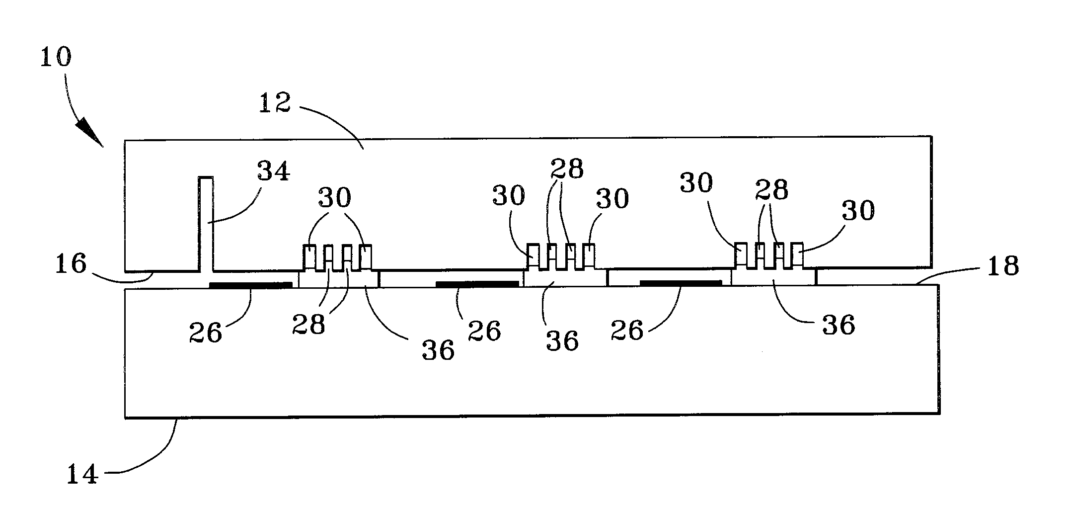
[0028]FIGS. 3 through 11 represent embodiments of the invention by which electrical shorting of wafer bonding structures with neighboring conductive device and / or circuit elements can be minimized if not eliminated during a wafer bonding process. FIGS. 3 through 5 represent a first embodiment in which electrical shorting of bonding structures 36 with neighboring electrodes 26 on a CMOS wafer 14 can be minimized if not eliminated by the presence of reservoirs 28 and barriers 30 defined in a device (for example, MEMS) wafer 12 that is mated and bonded to the CMOS wafer 14 using a metal bonding method, such as (but not limited to) solder bonding, transient liquid phase (TLP) bonding, and eutectic bonding, to form a wafer stack 10 shown in FIG. 5. The invention will be described in particular reference to Au—Si eutectic bonding, though other metal bonding system...


PUM

PropertyMeasurementUnit
Radiusaaaaaaaaaa
Pressureaaaaaaaaaa
Massaaaaaaaaaa

Abstract

A wafer bonding process that compensates for curvatures in wafer surfaces, and a wafer stack produced by the bonding process. The process entails forming a groove in a surface of a first wafer, depositing a bonding stack on a surface of a second wafer, aligning and mating the first and second wafers so that the bonding stack on the second wafer contacts a bonding site on the first wafer, and then heating the first and second wafers to reflow the bonding stack. The groove either surrounds the bonding site or lies entirely within the bonding site, and the heating step forms a molten bonding material, causes at least a portion of the molten bonding material to flow into the groove, and forms a bonding structure that bonds the second wafer to the first wafer. Bonding stacks having different lateral surface areas can be deposited to form bonding structures of different heights to compensate for variations in the wafer gap.

Description

CROSS REFERENCE TO RELATED APPLICATIONS[0001]This application claims the benefit of U.S. Provisional Application No. 61 / 194,090, filed Sep. 24, 2008, the contents of which are incorporated herein by reference.STATEMENT REGARDING FEDERALLY SPONSORED RESEARCH[0002]This invention was made with government support under Contract No. FA8650-07-C-1184 awarded by US Air Force. The Government has certain rights in the invention.BACKGROUND OF THE INVENTION[0003]The present invention generally relates to the fabrication and bonding of wafers, such as wafers for integrated circuit (IC) devices. More particularly, this invention relates to processes and bonding pad structures capable of compensating for nonplanarities in wafer surfaces.[0004]The fabrication of MEMS (microelectromechanical systems) devices typically entails bulk micromachining, surface machining, or combinations of the two to produce a three-dimensional (3-D) sensing structure. A MEMS device is often integrated with one or more C...

Claims


Application Information

Patent Timeline
IPC IPC(8): H01L27/12H01L21/98H01L21/18B23K31/00
CPCH01L21/187H01L25/50H01L2924/0002H01L2924/00
Inventor MENG, GUANGQINGZHANG, YAFANYAZDI, NAVID
Owner MICRO INERTIAL LLC
Why Eureka
Try Eureka