Semiconductor device and method of manufacturing the same

a technology of semiconductor devices and semiconductors, applied in semiconductor devices, semiconductor/solid-state device details, electrical apparatus, etc., can solve the problems of resistance of the interconnect against electromigration may degrade, and the adhesiveness between the metal interconnect and the barrier film may degrade, so as to reduce the degradation of the resistance to electromigration resistance, the effect of reducing the degradation of the adhesiveness and reducing the degradation of the resistan

a technology of semiconductor devices and semiconductors, applied in semiconductor devices, semiconductor/solid-state device details, electrical apparatus, etc., can solve the problems of resistance of the interconnect against electromigration may degrade, and the adhesiveness between the metal interconnect and the barrier film may degrade, so as to reduce the degradation of the resistance to electromigration resistance, the effect of reducing the degradation of the adhesiveness and reducing the degradation of the resistan

US20100078820A1Inactive Publication Date: 2010-04-01RENESAS ELECTRONICS CORP

Image

  • Semiconductor device and method of manufacturing the same
  • Semiconductor device and method of manufacturing the same
  • Semiconductor device and method of manufacturing the same

Examples


Embodiment Construction

[0020]The invention will now be described herein with reference to an illustrative embodiment. Those skilled in the art will recognize that many alternative embodiments can be accomplished using the teachings of the present invention and that the invention is not limited to the embodiments illustrated for explanatory purposes.

[0021]Embodiments of the present invention will be described below, referring to the attached drawings. Note that any similar constituents in all drawings will be given with similar reference numerals or symbols, and explanations therefor will not be repeated.

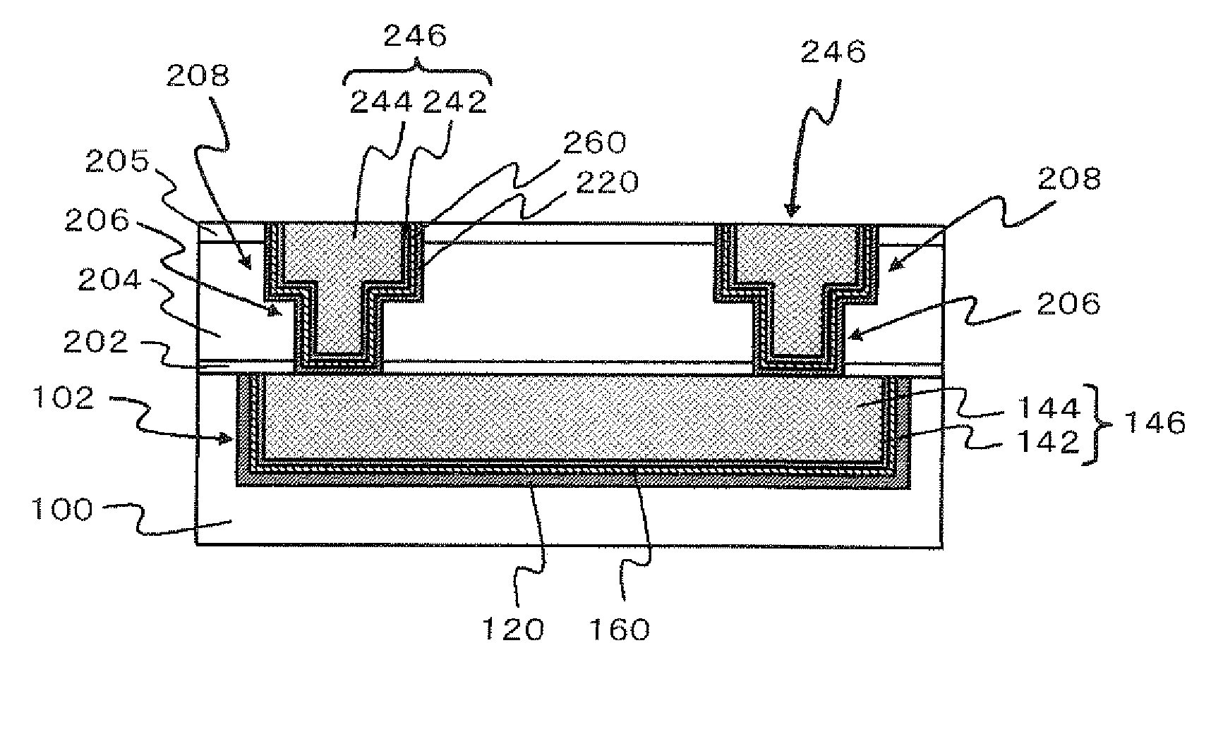
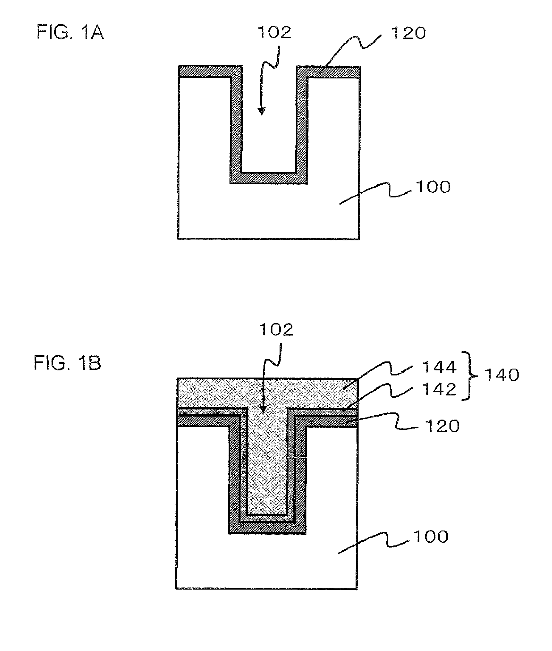
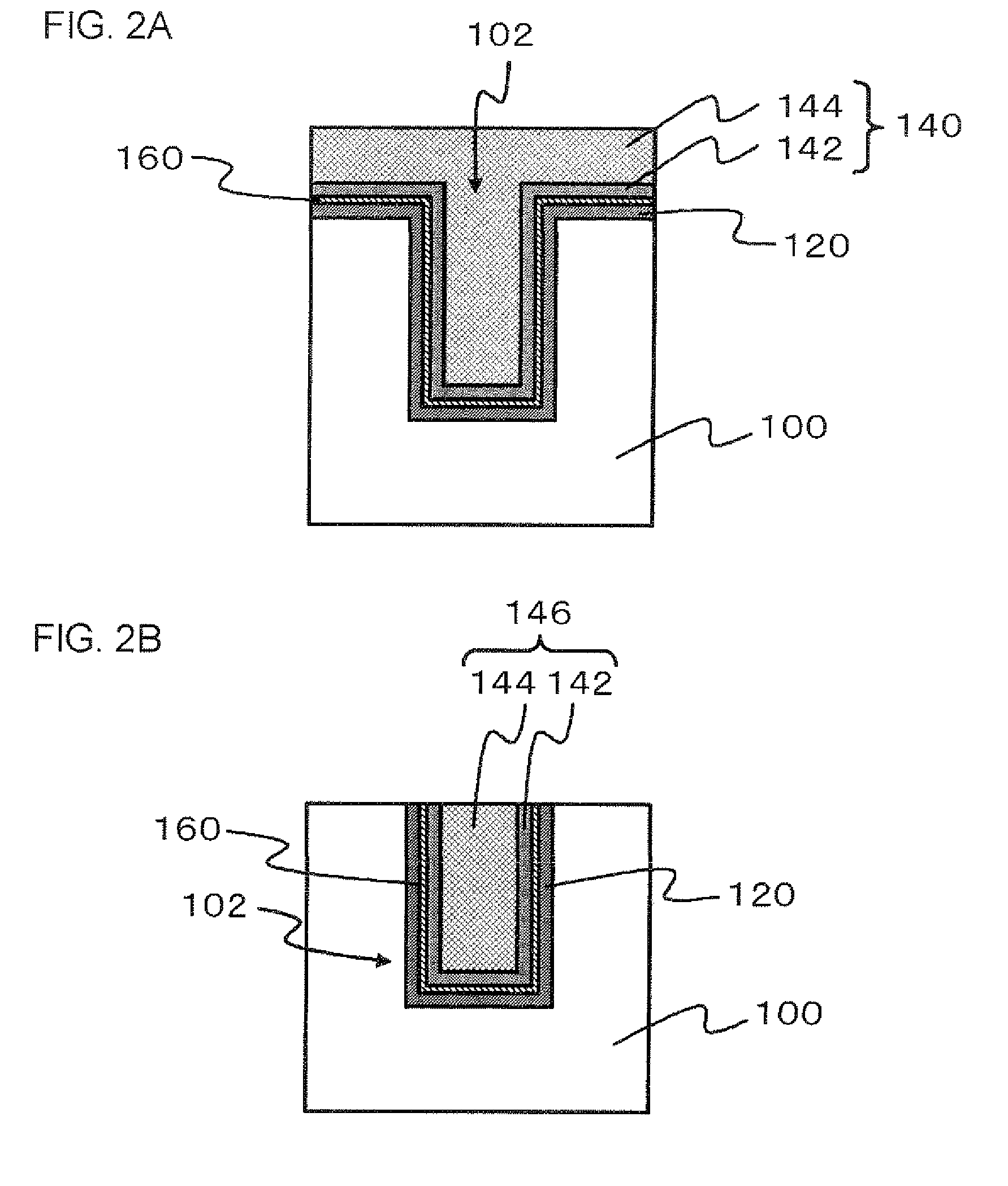
[0022]FIGS. 1A, 1B, 2A and 2B are sectional views explaining method of manufacturing a semiconductor device according to a first embodiment. The method of manufacturing a semiconductor device has steps described below. First, a trench 102 is formed in an insulating film 100 formed over a semiconductor substrate (not illustrated). Next, a metal barrier film 120 containing an additive element is formed on th...


PUM

PropertyMeasurementUnit
thicknessaaaaaaaaaa
thicknessaaaaaaaaaa
temperatureaaaaaaaaaa

Abstract

A metal barrier film which contains an additive element is formed on the side face and on the bottom of a trench formed in an insulating film; a seed film is formed over the metal barrier film; a plated layer (Cu film) is formed using the seed film as a seed so as to fill up the trench with a metal film; the metal barrier film and the metal film are annealed to thereby form therebetween an alloy layer which contains a metal composing the metal barrier film, the additive element, and a metal composing the metal film, and to thereby allow the additive element to diffuse into the metal film.

Description

[0001]This application is based on Japanese patent application No. 2008-252455 the content of which is incorporated hereinto by reference.BACKGROUND[0002]1. Technical Field[0003]The present invention relates to a semiconductor device which has an interconnect buried in an insulating film, and a method of manufacturing the same.[0004]2. Related Art[0005]There has been known an interconnect structure of semiconductor devices, configured to fill up a trench, which is formed in an insulating film, with an electro-conductive layer (Cu layer, for example). In thus-configured interconnect, there is provided a barrier film (diffusion preventive film) between the interconnect and the insulating film, aimed at preventing a metal composing the electro-conductive layer from diffusing into the insulating film. Provision of the barrier film raises a need of ensuring adhesiveness between the interconnect and the barrier film. On the other hand, the interconnect is in need of addition of an impurit...

Claims


Application Information

Patent Timeline
01 Apr 2010
Publication
US20100078820A1
IPC
H01L23/532; H01L21/768
CPC
H01L21/76843; H01L21/76846; H01L21/76858; H01L23/53295; H01L21/76883; H01L23/53238; H01L21/76873; H01L2924/0002
Inventors
KUROKAWA, TETSUYA; TOHARA, MAKOTO