AI technical title is built by Patsnap AI team. It summarizes the technical point description of the patent document.
a technology of nh4-nf3 and etching method, which is applied in the direction of semiconductor devices, semiconductor/solid-state device testing/measurement, decorative arts, etc., can solve the problems of native oxide contamination during etching, difficulty in processing, and undesirable native oxides
Active Publication Date: 2010-04-15
APPLIED MATERIALS INC
View PDF31 Cites 229 Cited by
Summary
Abstract
Description
Claims
Application Information
AI Technical Summary
This helps you quickly interpret patents by identifying the three key elements:
Problems solved by technology
Method used
Benefits of technology
Benefits of technology
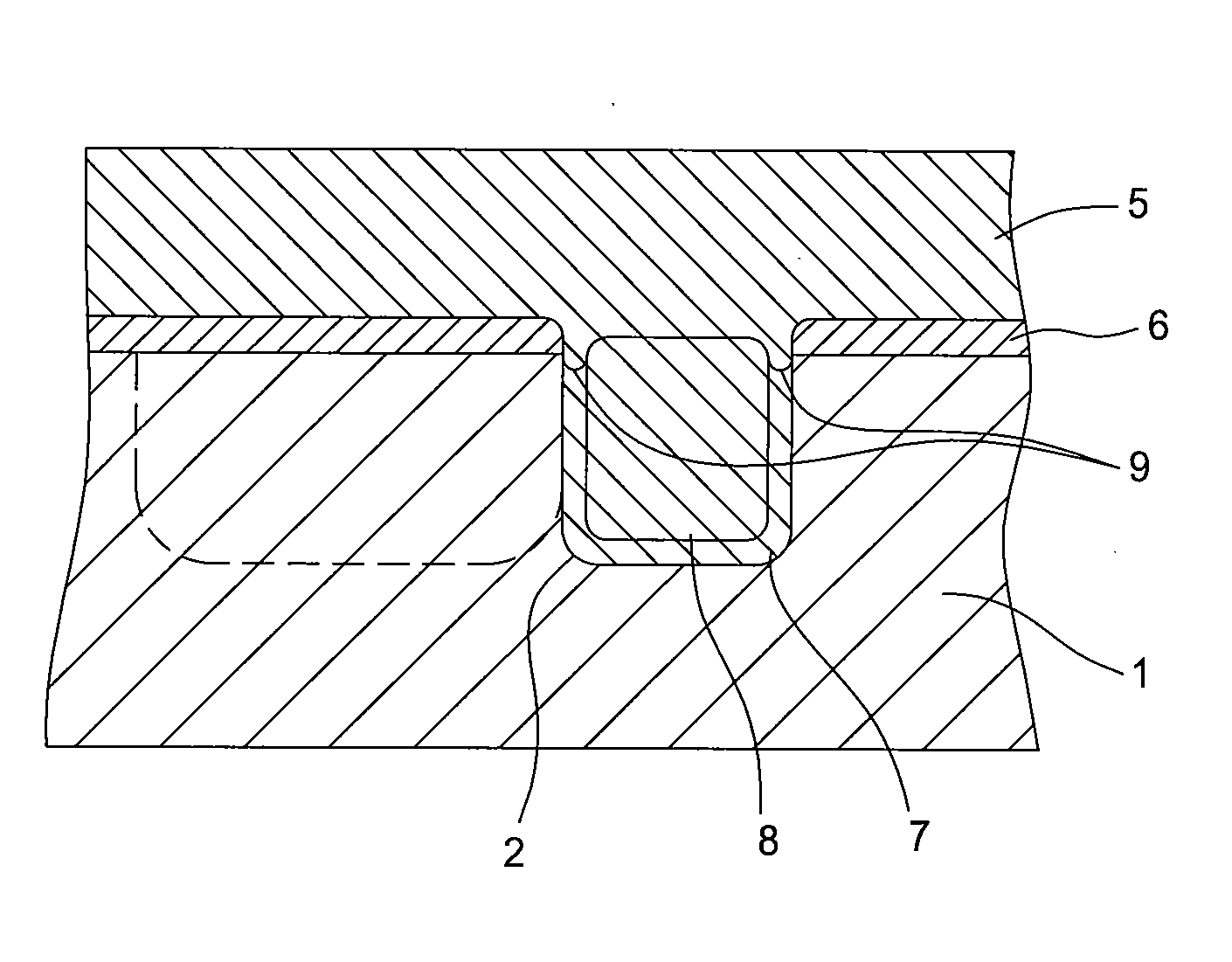
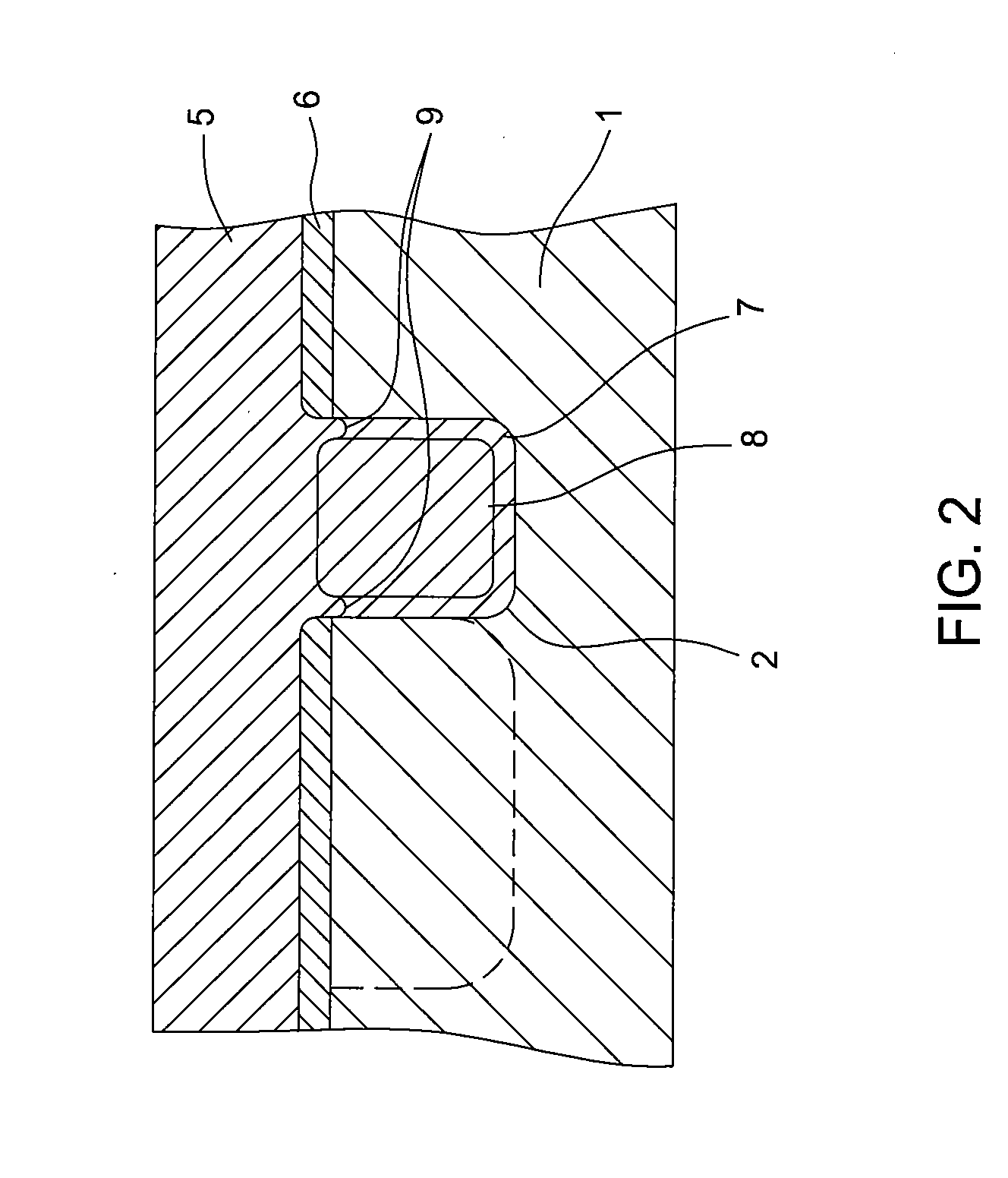
[0018]Yet another embodiment of the present invention provides a method for processing a substrate comprising positioning the substrate in a vacuum chamber, wherein the substrate having a surface feature comprising a first oxide and a second oxide, introducing an etching gas mixture to the vacuum chamber, generating active species from the etching gas mixture, at least partially reducing the first oxide by exposing the surface feature to the plasma of the etching gas mixture, and reducing the second oxide by an aqueous etch process.
Problems solved by technology
Native oxides may also result from contamination during etching.
Native oxides are typically undesirable and need to be removed prior to a subsequent process.
Some oxide features may have two or more oxides that respond differently to the same process, hence posing difficulties in processing, especially when feature sizes are smaller.
However, sputter etching process generally cannot completely remove oxides and can damage delicate silicon layers by physical bombardment.
However, diluted HF has the disadvantage of having a variable oxide etch rate.
This causes significant variability and integration issues in the process flow.
In reality various process variabilities cause significant unwanted leakages which contribute to the main current flow from source to drain.
Polysilicon wraps around inside the trench causes unwanted leakage and yield loss.
Method used
Image
Click on the blue label to locate the original text in one second.
Reading with bidirectional positioning of images and text.
Examples
example
[0080]During etching, a gas mixture of 2 sccm of NF3, 10 sccm of NH3 and 2,500 sccm of argon was introduced into a vacuum chamber, such as the processing chamber 100. A plasma of the gas mixture was ignited using 100 Watts of power. The bottom purge was 1,500 sccm of argon and the edge purge was 50 sccm of argon. The chamber pressure was maintained at about 6 Torr, and the substrate temperature was about 22° C. The substrate was etched for 120 seconds.
[0081]During anneal, the spacing was 750 mil and the lid temperature was 120° C. The substrate was annealed for about 60 seconds. About 50 angstroms of material was removed from the substrate surface. No anneal effect was observed. The etch rate was about 0.46 angstroms per second (28 Å / min). The observed etch uniformity was about 5% for the 50 Å etch.
[0082]Unless otherwise indicated, all numbers expressing quantities of ingredients, properties, reaction conditions, and so forth, used in the specification and claims are to be understoo...
PUM
Property
Measurement
Unit
temperature
aaaaa
aaaaa
temperature
aaaaa
aaaaa
temperature
aaaaa
aaaaa
Abstract
The present invention generally provides apparatus and methods for selectively removing various oxides on a semiconductor substrate. One embodiment of the invention provides a method for selectively removing an oxide on a substrate at a desired removal rate using an etching gas mixture. The etching gas mixture comprises a first gas and a second gas, and a ratio of the first gas and a second gas is determined by the desired removal rate.
Description
CROSS-REFERENCE TO RELATED APPLICATIONS[0001]This application is continuation of U.S. patent application Ser. No. 11 / 622,437 (Attorney Docket No. 8802 P2), filed Jan. 11, 2007.[0002]This application is also related to U.S. patent application Ser. No. 11 / 137,609 (Attorney Docket No. 8802 D1), filed May 24, 2005, now issued as U.S. Pat. No. 7,396,480; U.S. patent application Ser. No. 11 / 063,645 (Attorney Docket No. 8802), filed Feb. 22, 2005; U.S. patent application Ser. No. 11 / 137,199 (Attorney Docket No. 8802 D3), filed May 24, 2005; U.S. patent application Ser. No. 11 / 266,167 (Attorney Docket No. 8802 P1), filed Nov. 3, 2005; U.S. patent application Ser. No. 11 / 962,791 (Attorney Docket No. 8802 P3), filed Dec. 21, 2007; and U.S. patent application Ser. No. 12 / 134,715 (Attorney Docket No. 8802 C1), filed Jun. 6, 2008.BACKGROUND OF THE INVENTION[0003]1. Field of the Invention[0004]Embodiments of the present invention generally relate to methods and apparatus for processing semiconduc...
Claims
Application Information
Patent Timeline
Application Date:The date an application was filed.
Publication Date:The date a patent or application was officially published.
First Publication Date:The earliest publication date of a patent with the same application number.
Issue Date:Publication date of the patent grant document.
PCT Entry Date:The Entry date of PCT National Phase.
Estimated Expiry Date:The statutory expiry date of a patent right according to the Patent Law, and it is the longest term of protection that the patent right can achieve without the termination of the patent right due to other reasons(Term extension factor has been taken into account ).
Invalid Date:Actual expiry date is based on effective date or publication date of legal transaction data of invalid patent.
Patent Type & AuthorityApplications(United States)

