Long-range surface plasmon optical waveguide sensor

a technology of optical waveguide and long-range surface plasmon, which is applied in the direction of optical elements, superconductor devices, instruments, etc., can solve the problem of very short propagation distance of surface plasmon, and achieve the effect of effectively controlling the propagation characteristics of long-range surface plasmon, reducing loss of electromagnetic waves, and increasing detection sensitivity and limitation

Inactive Publication Date: 2010-04-22
IUCF HYU (IND UNIV COOP FOUND HANYANG UNIV)
View PDF10 Cites 17 Cited by
  • Summary
  • Abstract
  • Description
  • Claims
  • Application Information

AI Technical Summary

Benefits of technology

[0017]According to the present invention, it is possible to fabricate a long-range surface plasmon optical waveguide sensor, which can effectively control the propagating characteristics of a long-range surface plasmon. Also, loss of an electromagnetic wave is reduced, sensitivity and limitation of detection are increased and a high analysis speed is ensured. In addition, it is possible to fabricate a sensor of various sizes such as a small-sized or lightweight system, etc.

Problems solved by technology

Such a structure has a disadvantage in that since it allows the surface plasmon to be formed only on the surface of the metallic thin film, the surface plasmon propagates within a very short distance.

Method used


Image

  • Long-range surface plasmon optical waveguide sensor
  • Long-range surface plasmon optical waveguide sensor
  • Long-range surface plasmon optical waveguide sensor

Examples


Embodiment Construction

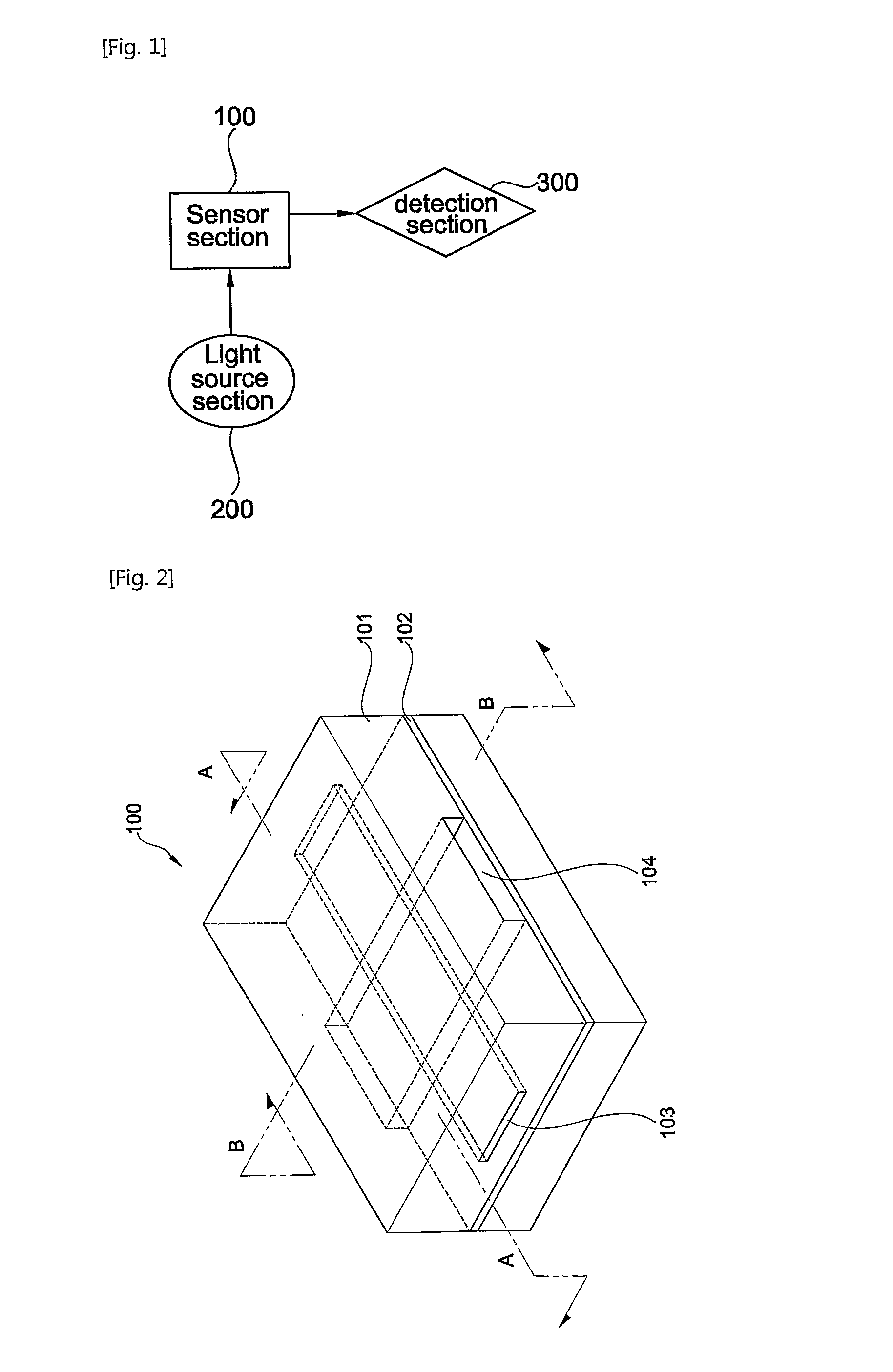
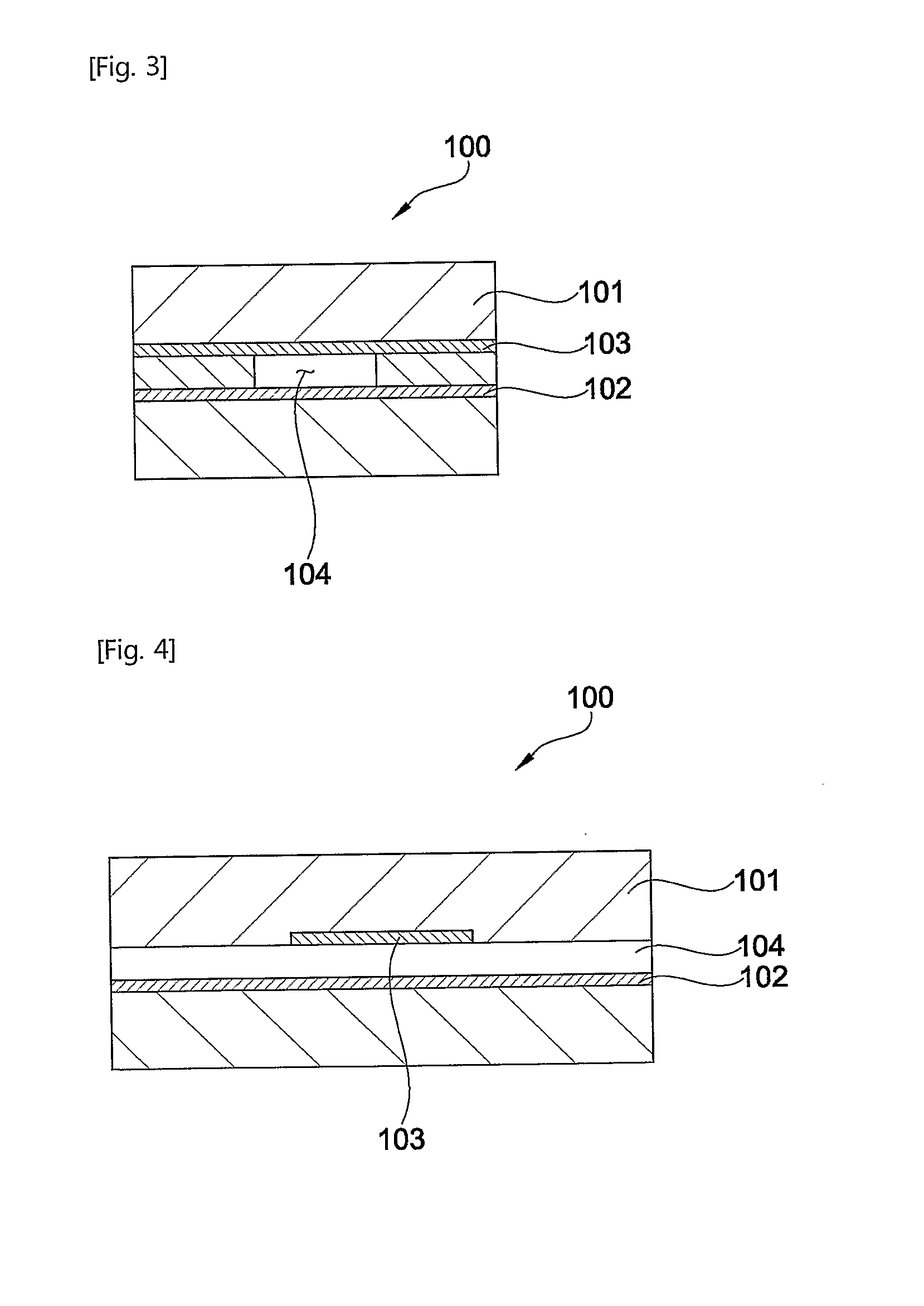
[0029]Reference will now be made in detail to the preferred embodiment of the present invention with reference to the attached drawings. The embodiments of the present invention can be modified in various other forms and should not be construed as being limited by or to the embodiments which will be described in detail hereinafter. Also, in the drawing preferably, the thickness, the size and the like of each element are not to scale and may be exaggerated for sake of explanation and clarity. In this case, throughout the drawings, like reference numerals are used to designate the same or similar elements although these elements are illustrated in different figures. Meanwhile, in case where it is described that one film is disposed “on” another film or a substrate, the one film may directly contact the other film or the substrate, or a third intervening film may be disposed between the one film and the other film or the substrate.

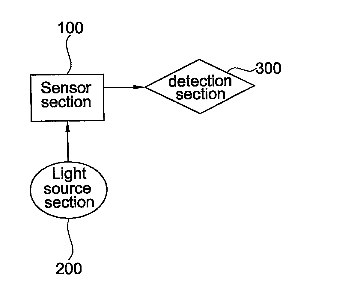
[0030]FIG. 1 is a block diagram showing the constructio...


PUM

PropertyMeasurementUnit
thicknessaaaaaaaaaa
thicknessaaaaaaaaaa
widthaaaaaaaaaa

Abstract

The present invention provides a long-range surface plasmon optical waveguide sensor which has a reduced loss of an electromagnetic wave, an increased sensitivity and limitation of detection and a high analysis speed, and enables fabrication of a sensor of various sizes such as a small-sized or lightweight system, etc. To this end, the long-range surface plasmon optical waveguide sensor, comprising: a sensor section, wherein the sensor section comprises a substrate, a first dielectric layer stacked on the substrate, a metal thin film stacked on the first dielectric layer, a second dielectric layer stacked on the metal thin film and having a channel penetratingly formed therein in such a fashion that the top surface of the metal thin film is partially exposed into the channel, a metal strip stacked on the second dielectric layer in such a fashion that the underside thereof is partially exposed into the channel, and a third dielectric layer stacked on the metal strip; a light source section for inducing a surface plasmon resonance between the metal thin film and the metal strip; and a detection section for detecting and analyzing a change of light according to the surface plasmon resonance.

Description

TECHNICAL FIELD[0001]The present invention relates to a long-range surface plasmon optical waveguide sensor, and more particularly, to a long-range surface plasmon optical waveguide sensor which has a reduced loss of an electromagnetic wave, an increased sensitivity and limitation of detection and a high analysis speed, and can be applied as a sensor of various sizes such as a small-sized or lightweight system, etc.BACKGROUND ART[0002]A surface plasmon refers to a fluctuation in the electron density, i.e., a collective vibration of an electron gas (or plasma) at the boundary surface of two materials of which real number terms of complex dielectric constants have opposite signs to each other. In this case, a surface plasmon wave generated by the surface plasmon is a surface electromagnetic wave propagating along the boundary surface between the two materials, i.e., a metal and a dielectric medium. The surface plasmon exists at the boundary surface between the metal having a negative ...

Claims


Application Information

Patent Timeline
Patent Type & Authority Applications(United States)
IPC IPC(8): G01N21/55
CPCG01N21/7703G01N21/553G01N21/27G01N33/48G01N2291/0256
Inventor SONG, SEOK HO
Owner IUCF HYU (IND UNIV COOP FOUND HANYANG UNIV)
Why Eureka
Try Eureka