Electronic component embedded printed circuit board and manufacturing method thereof

a technology of printed circuit board and electronic components, applied in the direction of printed circuit, printed circuit aspects, printed electric component incorporation, etc., can solve the problems of increasing the plating process and the time to plate, and achieve the effect of easy and reliable mounting and shortening the manufacturing tim

Inactive Publication Date: 2010-04-29
SAMSUNG ELECTRO MECHANICS CO LTD
View PDF2 Cites 9 Cited by
  • Summary
  • Abstract
  • Description
  • Claims
  • Application Information

AI Technical Summary

Benefits of technology

[0008]The present invention provides an electronic component embedded printed circuit board and a manufacturing method thereof, in which an electronic component without its electrode protruded outward can be mounted easily and reliably and the manufacturing time can be shortened.

Problems solved by technology

However, while forming the hole, it is possible to damage an electrode of the electronic component due to undercuts caused by the laser, thereby increasing the plating process and time to plate.

Method used


Image

  • Electronic component embedded printed circuit board and manufacturing method thereof
  • Electronic component embedded printed circuit board and manufacturing method thereof
  • Electronic component embedded printed circuit board and manufacturing method thereof

Examples


Embodiment Construction

[0021]As the invention allows for various changes and numerous embodiments, particular embodiments will be illustrated in the drawings and described in detail in the written description. However, this is not intended to limit the present invention to particular modes of practice, and it is to be appreciated that all changes, equivalents, and substitutes that do not depart from the spirit and technical scope of the present invention are encompassed in the present invention.

[0022]An electronic component embedded printed circuit board and a manufacturing method thereof in accordance with certain embodiments of the present invention will be described below in more detail with reference to the accompanying drawings. Those components that are the same or are in correspondence are rendered the same reference numeral regardless of the figure number, and redundant explanations are omitted.

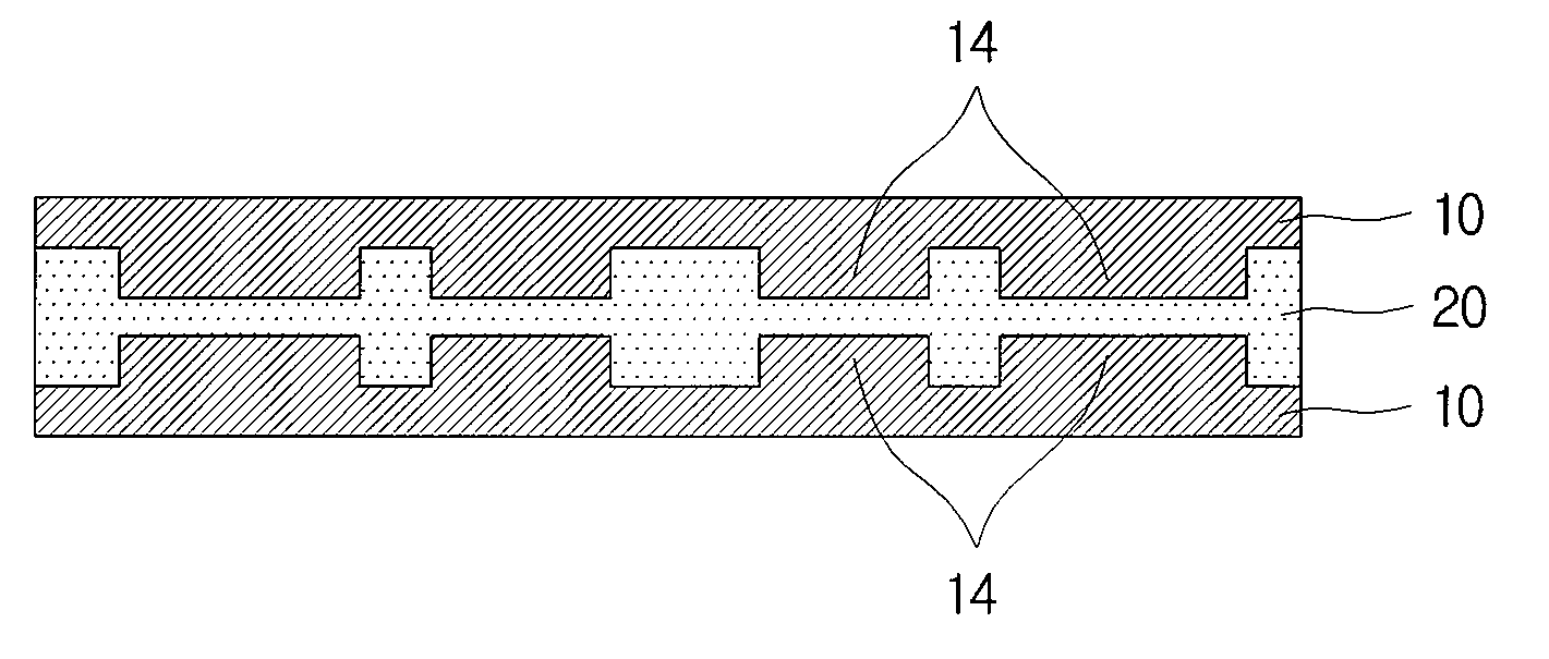
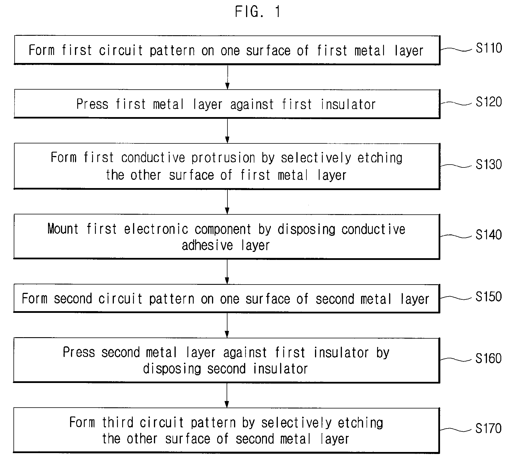
[0023]First of all, a method of manufacturing an electronic component embedded printed circuit board in ...


PUM

PropertyMeasurementUnit
conductiveaaaaaaaaaa
thicknessaaaaaaaaaa

Abstract

A printed circuit board with an electronic component embedded printed circuit board and a manufacturing method thereof are disclosed. According to an embodiment of the present invention, the method of manufacturing a printed circuit board with an embedded electronic component having a groove formed on one surface thereof and an electrode formed inside the groove includes: forming a first circuit pattern on one surface of a first metal layer; pressing the first metal layer against a first insulator; forming a first conductive protrusion by selectively etching the other surface of the first metal layer; and mounting a first electronic component by disposing a conductive adhesive layer such that an electrode of the first electronic component and the first conductive protrusion are electrically connected to each other. Thus, an electronic component without its electrode protruded outward can be mounted easily and reliably and the manufacturing time can be shortened.

Description

CROSS-REFERENCE TO RELATED APPLICATIONS[0001]This application claims the benefit of Korean Patent Application No. 10-2008-0105777, filed with the Korean Intellectual Property Office on Oct. 28, 2008, the disclosure of which is incorporated herein by reference in its entirety.BACKGROUND[0002]1. Technical Field[0003]The present invention relates to an electronic component embedded printed circuit board and a manufacturing method thereof.[0004]2. Description of the Related Art[0005]In step with the rapidly-changing information age, there has been an evolution of technologies in electronic component embedded printed circuit boards, in which various active components are not mounted on a surface of the printed circuit board but mounted inside the board, to provide more features in a small space. As more active components are increasingly embedded in the board, various functions of the various active components can be implemented and the lining of signaling can be minimized, thanks to the...

Claims


Application Information

Patent Timeline
Patent Type & Authority Applications(United States)
IPC IPC(8): H05K1/02H05K3/30
CPCH01L24/97Y10T29/49142H01L2924/01082H05K1/186H05K3/061H05K3/323H05K3/4652H05K2201/0367H05K2201/10674H05K2203/0152H05K2203/0376H05K2203/063H05K2203/1469H01L2924/01005H01L2924/01006H01L2924/01033Y10T29/49155Y10T29/49128Y10T29/49126Y10T29/4913Y10T29/49165H01L2924/01078H05K1/18
Inventor KIM, WOON-CHUNYIM, SOON-GYU
Owner SAMSUNG ELECTRO MECHANICS CO LTD
Why Eureka
Try Eureka