Semiconductor device and manufacturing method thereof

Active Publication Date: 2010-04-29
SEMICON COMPONENTS IND LLC
View PDF57 Cites 8 Cited by
  • Summary
  • Abstract
  • Description
  • Claims
  • Application Information

AI Technical Summary

Benefits of technology

[0015]The invention also provides a method of manufacturing a semiconductor device. The method includes providing a semiconductor substrate, forming a plurality of pad electrodes in a predetermined region on a top surface of the semiconductor substrate, bonding a supporter to the top surface of the semiconductor substrate using an adhesive, forming an opening in the semiconductor substrate at the predetermined region so as to penetrate through the

Problems solved by technology

In addition, the forming of the groove 123 has made the manufacturing process o

Method used


Image

  • Semiconductor device and manufacturing method thereof
  • Semiconductor device and manufacturing method thereof
  • Semiconductor device and manufacturing method thereof

Examples


Embodiment Construction

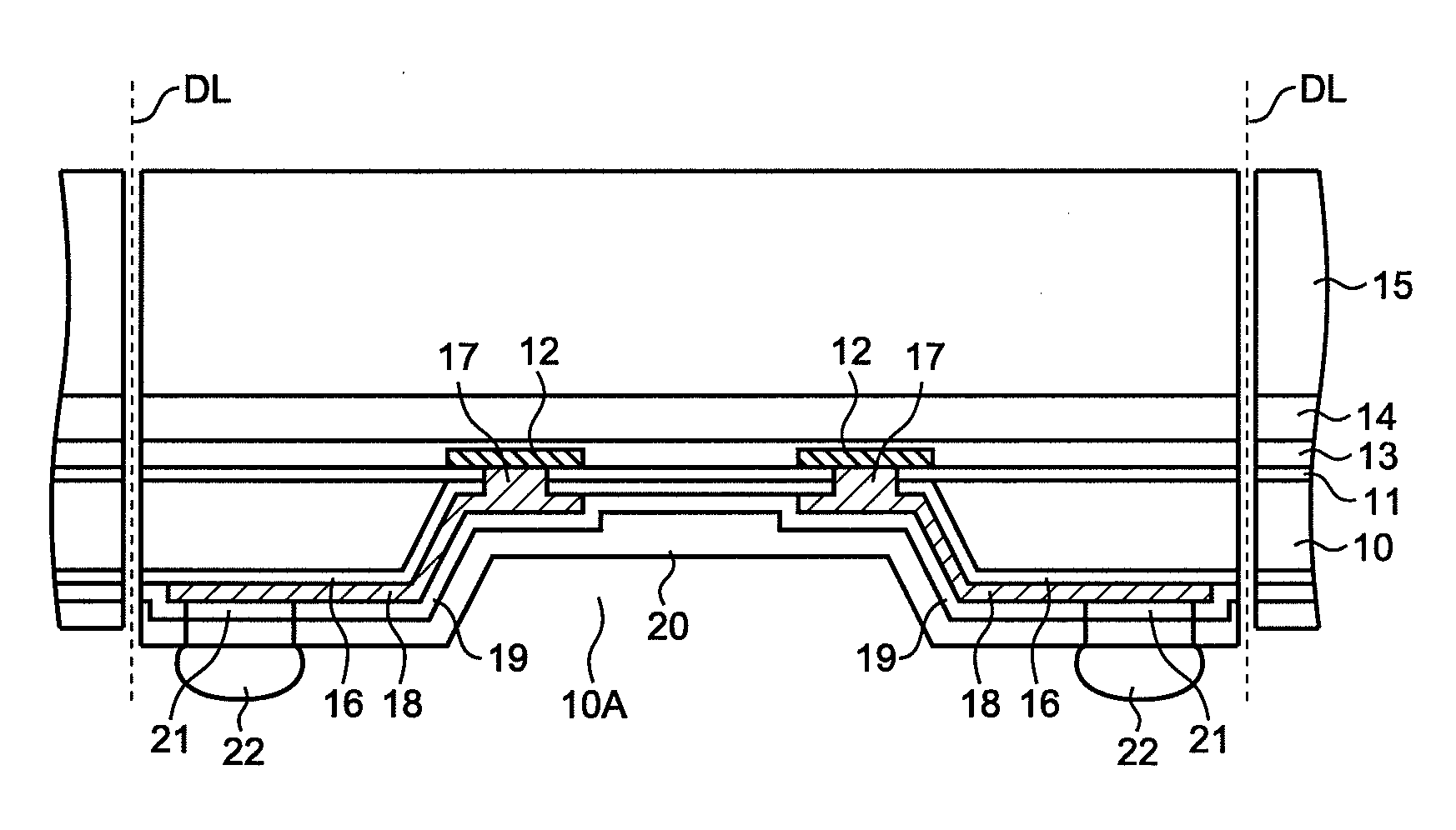
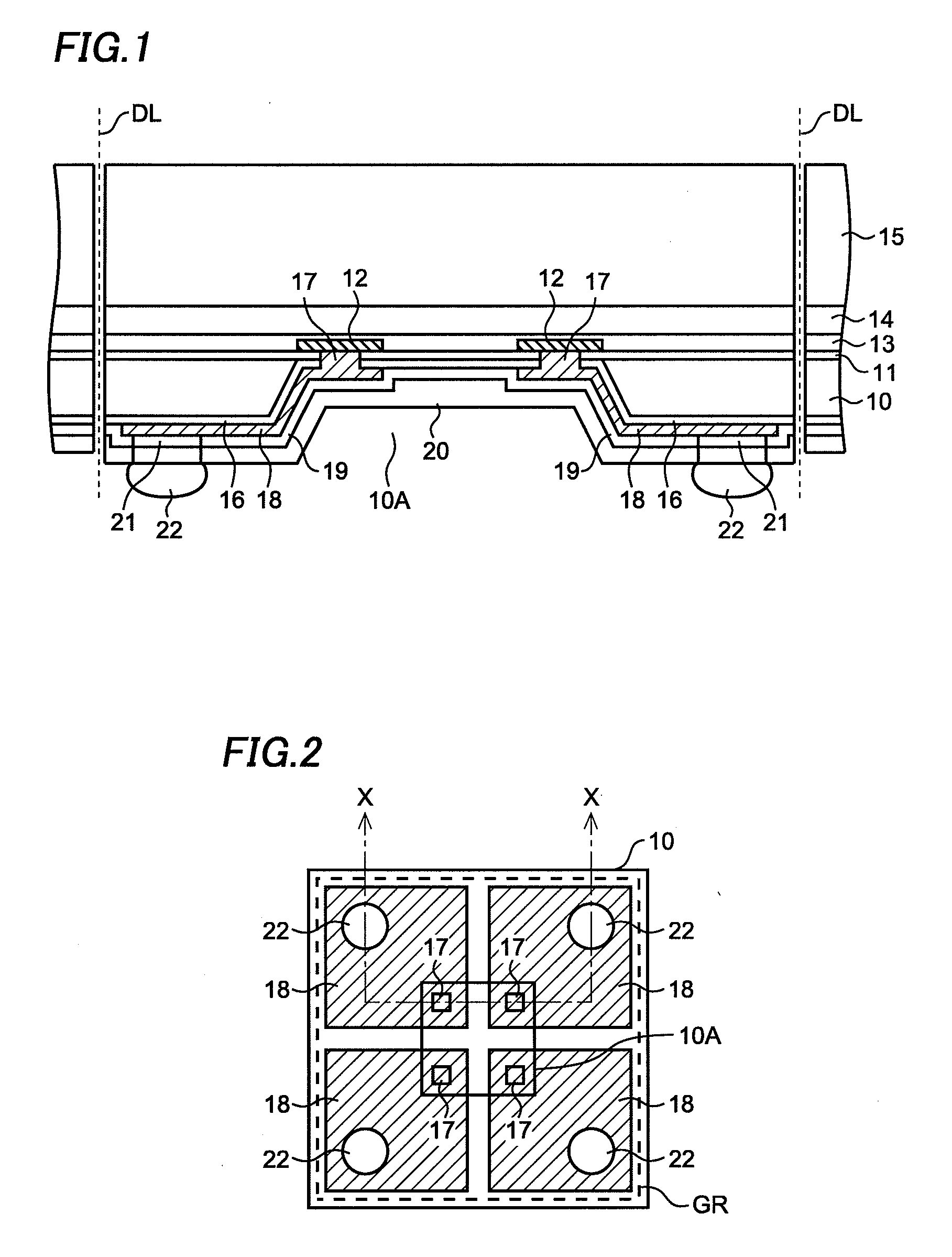
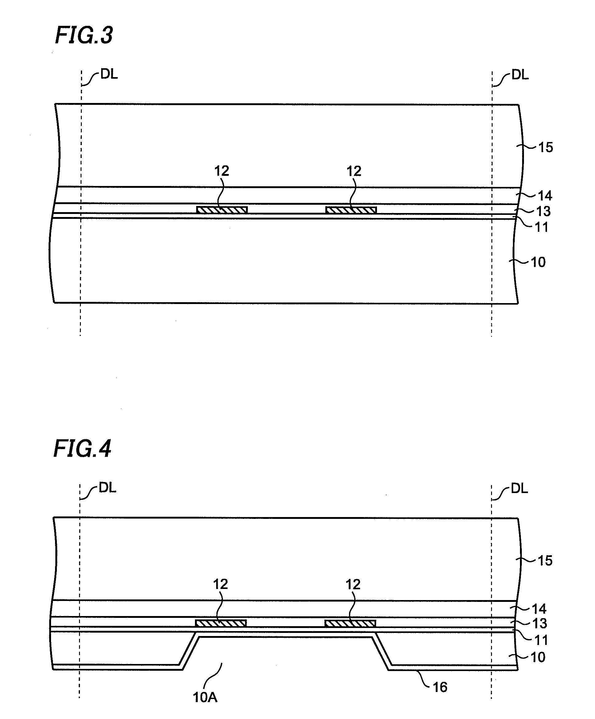
[0032]A semiconductor device according to an embodiment of this invention is hereafter described referring to the drawings. First, a structure of the semiconductor device will be described. FIG. 1 is a cross-sectional view showing the semiconductor device and its manufacturing method. FIG. 1 primarily shows one semiconductor device out of a plurality of the semiconductor devices formed in a wafer form of a semiconductor substrate 10. The cross-sectional view shown in FIG. 1 corresponds to a section X-X in an outline plan view shown in FIG. 2.

[0033]An insulation film 11 made of a BPSG (Boro-Phospho Silicate Glass) film or the like is disposed on a top surface of the semiconductor substrate 10 constituting the semiconductor device, and a plurality of pad electrodes 12 made of aluminum or the like is disposed on it, as shown in FIG. 1. The pad electrodes 12 may be made of aluminum and copper, or may be made of copper. The pad electrodes 12, each connected with an electronic device (not...


PUM


Abstract

A semiconductor device and its manufacturing method are offered to increase the number of semiconductor devices obtained from a semiconductor wafer while simplifying a manufacturing process. After forming a plurality of pad electrodes in a predetermined region on a top surface of a semiconductor substrate, a supporter is bonded to the top surface of the semiconductor substrate through an adhesive layer. Next, an opening is formed in the semiconductor substrate in a region overlapping the predetermined region. A wiring layer electrically connected with each of the pad electrodes is formed in the opening. After that, a stacked layer structure including the semiconductor substrate and the supporter is cut by dicing along a dicing line that is outside the opening.

Description

CROSS-REFERENCE OF THE INVENTION[0001]This application claims priority from Japanese Patent Application No. 2008-273229, the content of which is incorporated herein by reference in its entirety.BACKGROUND OF THE INVENTION[0002]1. Field of the Invention[0003]This invention relates to a semiconductor device and its manufacturing method, specifically to a chip size package and its manufacturing method.[0004]2. Description of the Related Art[0005]A CSP (Chip Size Package) has received attention in recent years as a new packaging technology. The CSP means a small package having about the same outside dimensions as those of a semiconductor die packaged in it.[0006]A BGA (Ball Grid Array) type semiconductor device is known as a kind of chip size package device. An example structure of the BGA type semiconductor device is described hereafter.[0007]A pad electrode 112 is disposed on an insulation film 111 disposed on a top surface of a semiconductor substrate 110 that constitutes the semicon...

Claims


Application Information

Patent Timeline
IPC IPC(8): H01L23/488H01L21/768H01L21/304
CPCH01L21/6835H01L2924/01006H01L21/78H01L23/481H01L24/02H01L24/12H01L2221/68372H01L2224/0401H01L2224/13144H01L2224/2518H01L2924/01004H01L2924/01013H01L2924/01014H01L2924/01029H01L2924/01033H01L2924/01047H01L2924/01078H01L2924/01079H01L2924/01082H01L2924/014H01L2924/05042H01L2924/10157H01L2924/3025H01L21/76898H01L2924/15788H01L2924/0001H01L2224/05569H01L2224/13024H01L2224/0236H01L2224/0235H01L2224/02377H01L2924/10156H01L2924/00H01L2224/02
Inventor TOMITA, HIROAKISUTOU, KAZUYUKI
Owner SEMICON COMPONENTS IND LLC
Why Eureka
Try Eureka