Magnetic Tunnel Junction and Memristor Apparatus

a technology of magneto-magnetic tunnel junction and magneto-magnetic tunnel junction, which is applied in the direction of bulk negative resistance effect devices, magnetic property measurements, instruments, etc., can solve the problems of limited endurance, slow access speed, and ns read

Inactive Publication Date: 2010-05-06
SEAGATE TECH LLC
View PDF19 Cites 34 Cited by
  • Summary
  • Abstract
  • Description
  • Claims
  • Application Information

AI Technical Summary

Benefits of technology

[0008]A further particular embodiment is a method of power consumed by an electrical device. The method includes passing current through a memristor solid state element and an electrical device. The memristor solid state element measures the current passing through the memristor solid state element and forms a memristance value. The memristor solid state el...

Problems solved by technology

Current devices using flash memory have several drawbacks such as slow access speed (˜ms write and ˜50-100 ns read), limited endurance (˜103-104 programming cycles), and the integration difficulty in system-on-ch...

Method used


Image

  • Magnetic Tunnel Junction and Memristor Apparatus
  • Magnetic Tunnel Junction and Memristor Apparatus
  • Magnetic Tunnel Junction and Memristor Apparatus

Examples


Embodiment Construction

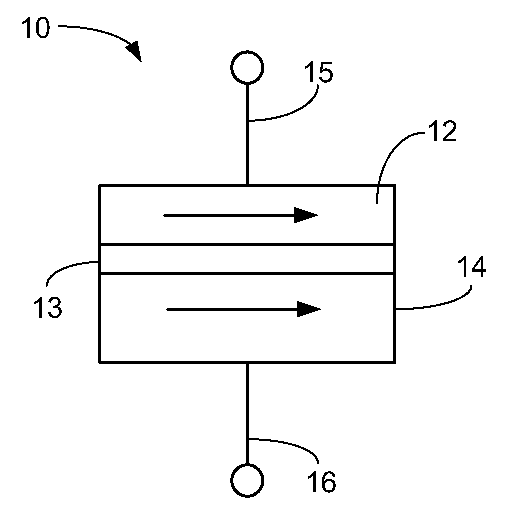
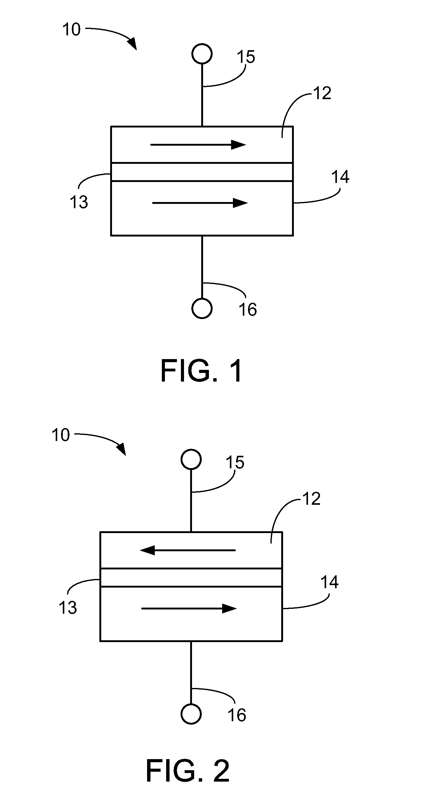
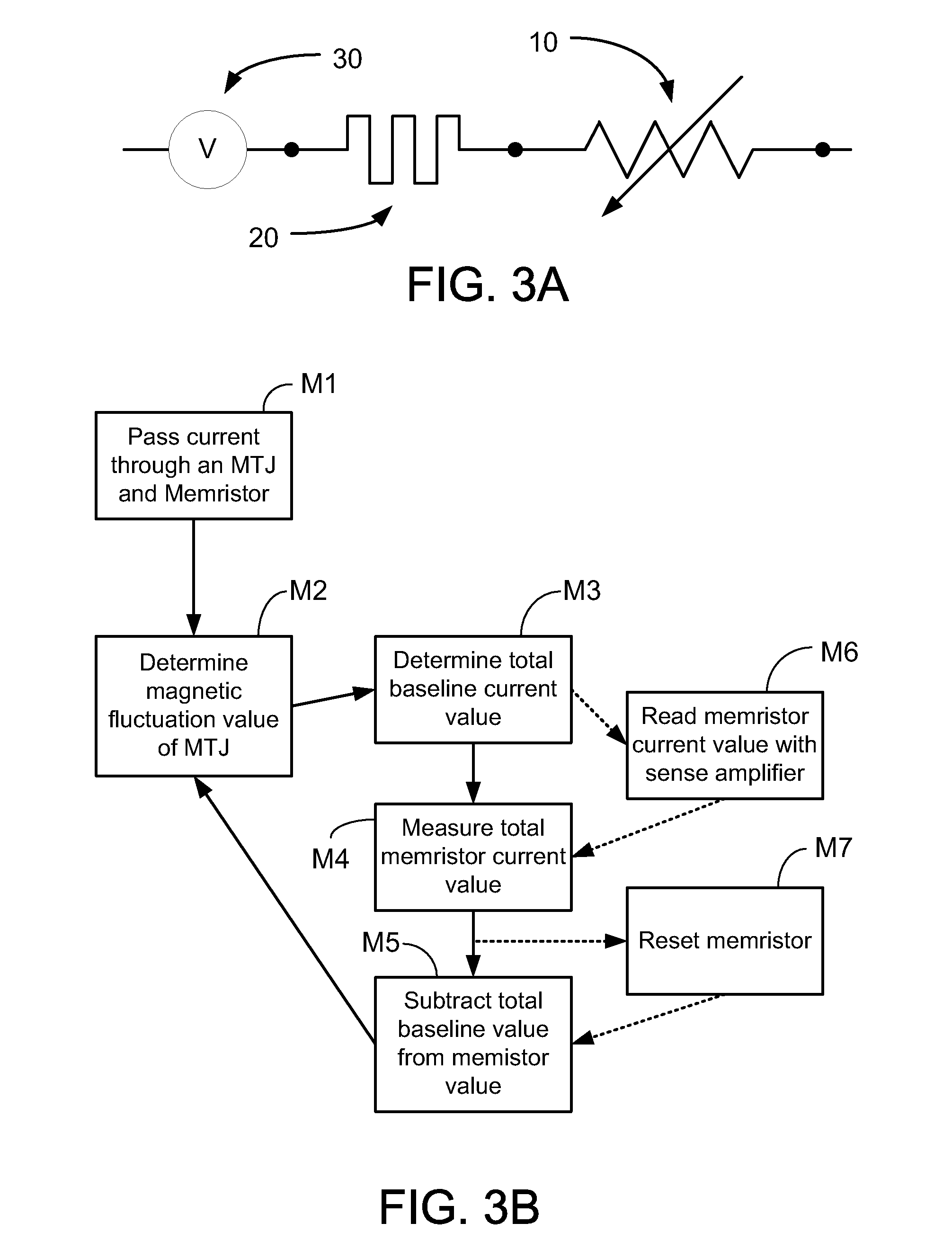
[0024]In the following description, reference is made to the accompanying set of drawings that form a part hereof and in which are shown by way of illustration several specific embodiments. It is to be understood that other embodiments are contemplated and may be made without departing from the scope or spirit of the present disclosure. The following detailed description, therefore, is not to be taken in a limiting sense. The definitions provided herein are to facilitate understanding of certain terms used frequently herein and are not meant to limit the scope of the present disclosure.

[0025]Unless otherwise indicated, all numbers expressing feature sizes, amounts, and physical properties used in the specification and claims are to be understood as being modified in all instances by the term “about.” Accordingly, unless indicated to the contrary, the numerical parameters set forth in the foregoing specification and attached claims are approximations that can vary depending upon the ...


PUM


Abstract

A magnetic memory device includes a magnetic tunnel junction having a free magnetic layer having a magnetization orientation that is switchable between a high resistance state magnetization orientation and a low resistance state magnetization orientation and a memristor solid state element electrically coupled to the magnetic tunnel junction. The memristor has a device response that is an integrated voltage versus an integrated current.

Description

CROSS-REFERENCE TO RELATED APPLICATIONS[0001]This application claims the benefit of U.S., Provisional Application No. 61 / 109,970 filed Oct. 31, 2008, the contents of which is hereby incorporated by reference in its entirety.BACKGROUND[0002]Fast growth of the pervasive computing and handheld / communication industry has generated exploding demand for electrical devices including high capacity nonvolatile solid-state data storage devices. Current devices using flash memory have several drawbacks such as slow access speed (˜ms write and ˜50-100 ns read), limited endurance (˜103-104 programming cycles), and the integration difficulty in system-on-chip (SoC). Flash memory (NAND or NOR) also faces significant scaling problems at 32 nm node and beyond.[0003]Magneto-resistive or magnetic random access memory (MRAM) is a promising candidate for future memory. One basic component of MRAM is a magnetic tunneling junction (MTJ). Data storage is realized by switching the resistance of MTJ between ...

Claims


Application Information

Patent Timeline
IPC IPC(8): G01R33/18H01L45/00
CPCG01R33/098G11C13/003G11C2213/56G11C11/1675H01L27/224H01L43/08G11C11/1673G11C2213/76H10B61/10H10N50/10
Inventor WANG, XIAOBINCHEN, YIRANWANG, ALANXI, HAIWENZHU, WENZHONGLI, HAILIU, HONGYUE
Owner SEAGATE TECH LLC
Why Eureka
Try Eureka