
Touch Screen Sensor

a capacitive touch screen and electrode layer technology, applied in the manufacture of printed circuits, instruments, printed circuit assembling, etc., can solve the problems of high resistance, high cost and time-consuming test stages, and relatively high percentage of films damaged, etc., to achieve low metal densities, high electrical conductivity, and low resistance.

Active Publication Date: 2010-05-20
BOE TECH GRP CO LTD
View PDF34 Cites 147 Cited by
  • Summary
  • Abstract
  • Description
  • Claims
  • Application Information

AI Technical Summary

Benefits of technology

[0008]As a result, a mesh of fine metal lines of about 10 μm width can be applied to a substrate such as PET film, which is 98% clear, better than ITO. The metal lines are so narrow as to be optically invisible. Also, the mesh configuration allows for robust performance, since a break in the metal is ‘cured’ by alternate paths around the defect. Furthermore, copper is malleable unlike ITO and can be readily flexed or kinked without damage. Unlike PEDOT, fine line copper has no problems with environmental deterioration under normal conditions of anticipated use.
[0015]Adjacent electrodes may be spaced apart by a plurality of islands also made of interconnected metal traces, the metal traces of the islands being visually and electrically similar to the metal traces of the electrodes. These islands in-fill between electrodes to provide visual continuity.

Problems solved by technology

ITO films are clear to about 92% (single layer), but have a relatively high resistance and are known to be quite fragile.
A relatively high percentage of films become damaged during production, requiring an expensive and time-consuming test stage.
Also, ITO films are expensive and there are only a few suppliers who can competently manufacture such films, causing logistical problems for users of these films.
Finally, Indium is a scarce metal which is increasingly in demand, yet production of this metal is limited by the few mines which produce it.
However PEDOT is not as optically clear as ITO, is difficult to deposit uniformly, and degrades rapidly under adverse environmental conditions.

Method used


Image

  • Touch Screen Sensor
  • Touch Screen Sensor
  • Touch Screen Sensor

Examples


Embodiment Construction

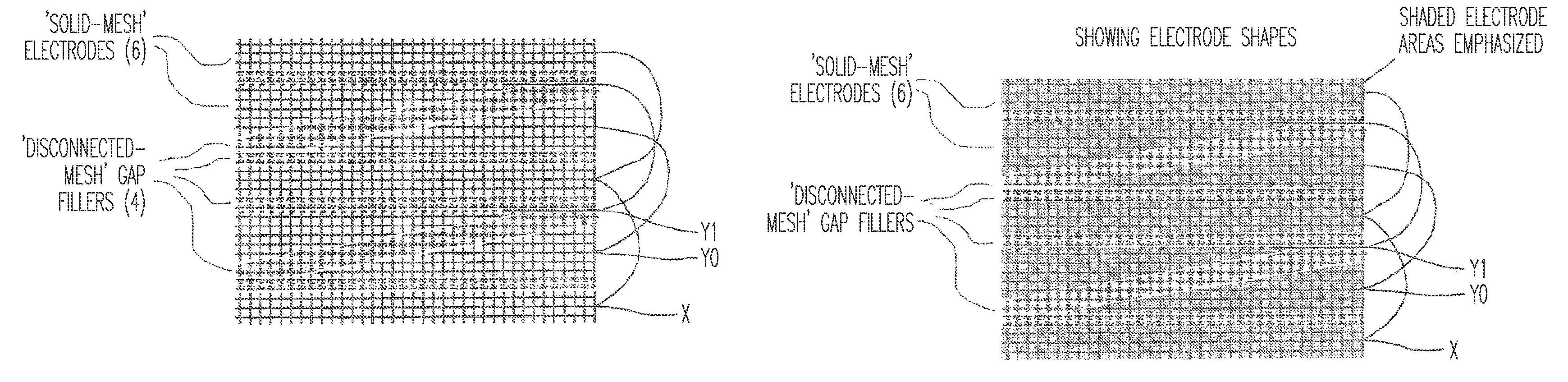
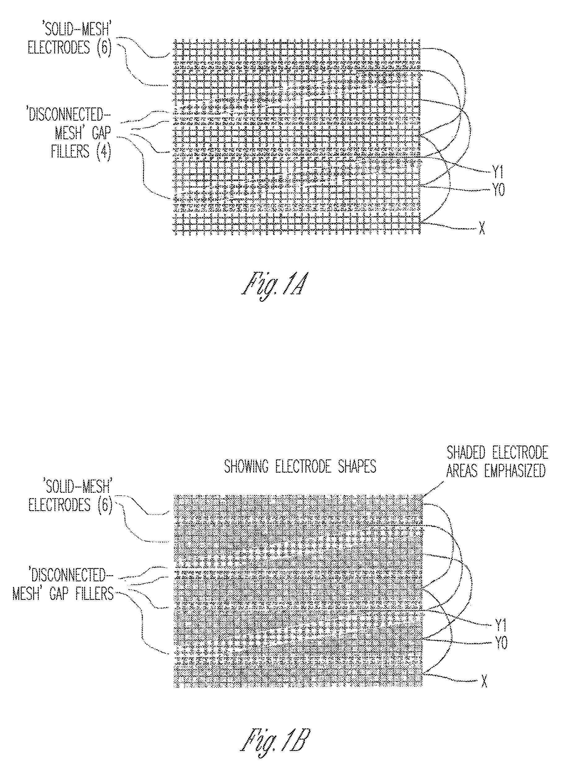
[0033]Processes have been recently developed which allow the printing of ultra-fine metal traces on plastic films and glass, as thin as 10 μm or even less. The metals used include copper, which is highly conductive and has a darker color than other metals, for example chrome. The technology has been developed using standard photolithographic processes and can be used to mass produce films on a roll-to-roll process for extremely low cost. No expensive, rare, or exotic materials are used in the manufacture of these metal traces. The technology has been developed specifically for use in micro-circuit applications, for example RFID tags, smart cards, displays, and the like.

[0034]These fine metal traces can also be used to develop field-emitting structures, using a sparse mesh configuration which has been shown to emit copious amounts of electric field, almost the same as a solid electrode shape. A sparse mesh allows for high optical clarity; if the traces are 10 μm or less, and the mesh...


PUM

PropertyMeasurementUnit
Fractionaaaaaaaaaa
Widthaaaaaaaaaa
Densityaaaaaaaaaa

Abstract

A two-dimensional touch sensor comprising a plurality of electrodes arranged in a mesh pattern on a substrate. Each electrode is formed by interconnected metal traces, the metal being intrinsically opaque, but the metal traces being sufficiently narrow to be practically invisible. The metal traces have a width less than or equal to 10 μm and occupy less than or equal to 5% of the area of each electrode. The electrodes can be deposited additively via a printing process, for example using copper as the metal. The narrow width of the tracks allows the film to be highly transparent, since the electric field used in capacitive touch screens can be made to propagate with very low metal densities.

Description

BACKGROUND OF THE INVENTION[0001]The present invention relates to the manufacture and application of capacitive touch screen electrode layers by the use of single layer fine-line metal mesh electrodes printed onto a substrate. The method includes a simple way to self-test the electrodes from a connector so as to avoid the need for more elaborate test methodologies.[0002]Most touch screens today, capacitive or otherwise, use a sputtered layer of Indium Tin Oxide (ITO) deposited onto a thin plastics film (such as PET film) or directly onto a glass layer. The ITO is uniformly deposited then etched using a subtractive process which involves numerous process steps. Finally, layers of silver ink and dielectric are used to make connections to the ITO on film or glass, which adds yet more process steps.[0003]ITO films are clear to about 92% (single layer), but have a relatively high resistance and are known to be quite fragile. A relatively high percentage of films become damaged during pro...

Claims


Application Information

Patent Timeline
IPC IPC(8): G06F3/041G06F19/00H05K3/30
CPCG06F3/044Y10T29/4913G06F2203/04112G06F3/0446G06F3/04166
Inventor PHILIPP, HARALD
Owner BOE TECH GRP CO LTD
Features
  • Generate Ideas
  • Intellectual Property
  • Life Sciences
  • Materials
  • Tech Scout
  • Unparalleled Data Quality
  • Higher Quality Content
  • 60% Fewer Hallucinations
Learn More