Bi-layer pseudo-spin field-effect transistor

a field-effect transistor and pseudo-spin technology, applied in the field of field-effect transistors, can solve the problems of increasing energy consumed during switching, inability to further scale supply voltage beyond, and improving speed and energy efficiency. , to achieve the effect of low gate and interlayer bias

Inactive Publication Date: 2010-05-27
BOARD OF RGT THE UNIV OF TEXAS SYST
View PDF7 Cites 58 Cited by
  • Summary
  • Abstract
  • Description
  • Claims
  • Application Information

AI Technical Summary

Benefits of technology

[0010]In accordance with a preferred embodiment of the present invention, a bi-layer pseudo-spin field-effect transistor (BiSFET) includes a first layer and a second layer separated by a tunnel d

Problems solved by technology

However, the energy consumed during switching increases according to the square of the supply voltage.
The inability to further scale supply voltages

Method used


Image

  • Bi-layer pseudo-spin field-effect transistor
  • Bi-layer pseudo-spin field-effect transistor
  • Bi-layer pseudo-spin field-effect transistor

Examples


Embodiment Construction

I. Introduction

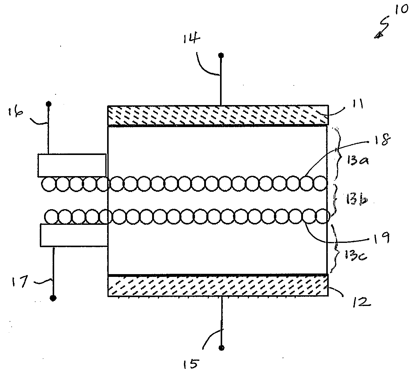
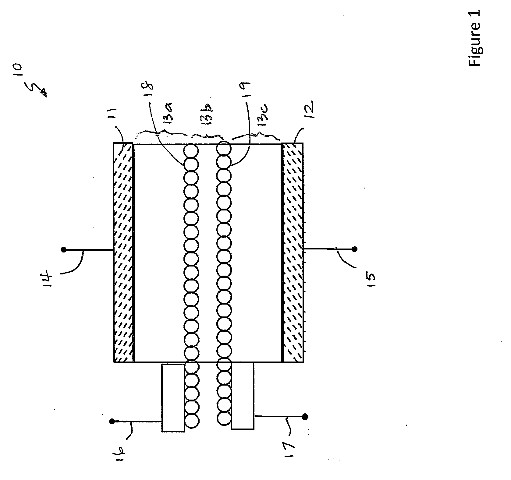
[0019]The present invention is a new type of transistor capable of consuming less power than conventional field-effect transistors (FETs). The new type of transistors, which can be called bi-layer pseudo-spin FETs (BiSFETs), are based on the concept of pseudo-spin in semiconductor bi-layers (or two quantum wells separated by a tunnel barrier), and the carriers in the bi-layers are controlled via two electrical gates. Pseudo-spin is a concept analogous to the quantum mechanical “spin” of an electron. Instead of an electron having spin “up” or “down” degree of freedom, pseudo-spin refers to the “which layer” degree of freedom.

II. Bi-Layer Pseudo-Spin Field Effect Transistor

[0020]Referring now to the drawings, and in particular to FIG. 1, there is depicted a diagram of a BiSFET, in accordance with a preferred embodiment of the present invention. As shown, a BiSFET 10 includes dielectric layers 13a, 13b and 13c formed between a first gate 11 and a second gate 12. A first ...


PUM


Abstract

A bi-layer pseudo-spin field-effect transistor (BiSFET) is disclosed. The BiSFET includes a first and second conduction layers separated by a tunnel dielectric. The BiSFET transistor also includes a first gate separated from the first conduction layer by an insulating dielectric layer, and a second gate separated from the second conduction layer by an insulating layer. These conduction layers may be composed of graphene. The voltages applied to the first and/or second gates can control the peak current and associated voltage value for current flow between top and bottom conduction channels, and interlayer current voltage characteristic exhibiting negative differential resistance. BiSFETs may be used to make a variety of logic gates. A clocked power supply scheme may be used to facilitate BiSFET-based logic.

Description

PRIORITY CLAIM[0001]The present application claims priority under 35 U.S.C. §119(e)(1) to provisional application No. 61 / 118,251 filed on Nov. 26, 2008, the contents of which are incorporated herein by reference.BACKGROUND OF THE INVENTION[0002]1. Technical Field[0003]The present invention relates to field-effect transistors in general, and in particular to bi-layer pseudo-spin field-effect transistors.[0004]2. Description of Related Art[0005]For a field-effect transistor (FET), a gate typically controls electrical current that flows between a source and a drain. In a metal-oxide semiconductor field-effect transistor (MOSFET), gate control is achieved by regulating the height of a conduction channel in energy below threshold or through self consistent electrostatics and the number of charge carriers within the conduction channel above a threshold, with the threshold being the point of switching between an ON state and an OFF state of the MOSFET. For a short-channel (i.e., a few tens...

Claims


Application Information

Patent Timeline
IPC IPC(8): H01L29/78
CPCB82Y10/00H01L29/1606H01L29/7831H01L29/7781H01L29/775
Inventor BANERJEE, SANJAY K.REGISTER, II, LEONARD FRANKLINMACDONALD, ALLANPALLE, DHARMENDAR REDDYTUTUC, EMMANUEL
Owner BOARD OF RGT THE UNIV OF TEXAS SYST
Why Eureka
Try Eureka