Multilayered through via

a through via and multi-layer technology, applied in the field of semiconductor through vias, can solve the problems of ineffective copper through vias, many difficulties, and inability to meet the requirements of front-end process preferred materials,

Inactive Publication Date: 2010-05-27
NXP USA INC
View PDF21 Cites 97 Cited by
  • Summary
  • Abstract
  • Description
  • Claims
  • Application Information

AI Technical Summary

Problems solved by technology

Many difficulties, however, remain.
One continuing problem is sufficiently filling the through via without forming voids.
This is a difficult issue due to the relatively long distance the through via must traverse in going from one side of a substrate to the other side.
Further, there are issues relating to compatibility with preferred materials used for front end processes.
Copper is commonly used for interconnect but use for vias, especially in contacting silicides, has provided problems.
Even though many deposition problems with plating copper have been overcome, copper has not been found to be effective for through vias due in part with incompatibility with the contact materials used for contacting silicides.
Also plating can be difficult in a via that is very small or has a high aspect ratio.

Method used


Image

  • Multilayered through via
  • Multilayered through via
  • Multilayered through via

Examples


Embodiment Construction

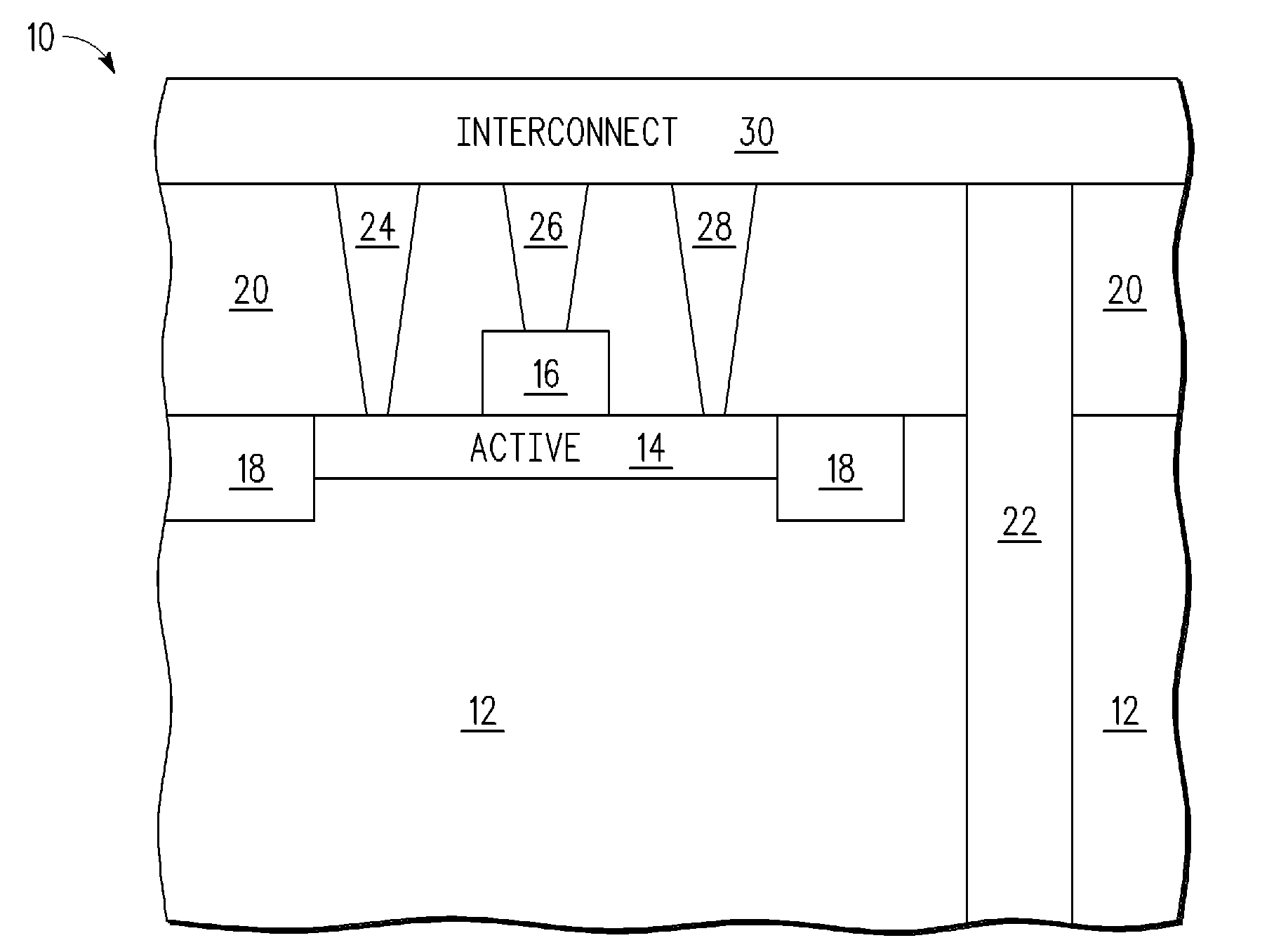
[0025]In one aspect, a through via is made by forming an opening in a substrate to a first depth, a first layer of titanium nitride is deposited to line the opening. A much thicker first layer of tungsten is deposited over the first layer of titanium nitride. After the deposition of the first layer of tungsten, a second layer of titanium nitride is deposited in the opening. After the deposition of the second layer of titanium nitride, a second layer of tungsten is deposited in the opening. As needed, an etch back of the first layer of tungsten may be etched back to remove tungsten at the top portion of the opening. Subsequent processing establishes contact to the tungsten in the opening, and a backgrind of the substrate is performed to expose tungsten at a bottom of the opening. Also it is beneficial to precede the first titanium nitride layer with a titanium layer. This is better understood by reference to the drawings and the following specification.

[0026]The semiconductor substra...


PUM

PropertyMeasurementUnit
thicknessaaaaaaaaaa
widthaaaaaaaaaa
widthaaaaaaaaaa

Abstract

A method for forming a through substrate via (TSV) comprises forming an opening within a substrate. An adhesion layer of titanium is formed within the via opening, a nucleation layer of titanium nitride is formed over the adhesion layer, and a tungsten layer is deposited over the nucleation layer, the tungsten layer having a thickness less than or equal to a critical film thickness sufficient to provide for film integrity and adhesion stability. A stress relief layer of titanium nitride is formed over the tungsten layer and a subsequent tungsten layer is deposited over the stress relief layer. The subsequent tungsten layer has a thickness less than or equal to the critical film thickness. The method further includes planarizing to expose the interlevel dielectric layer and a top of the TSV and backgrinding a bottom surface of the substrate sufficient to expose a bottom portion of the TSV.

Description

BACKGROUND [0001]1. Field[0002]This disclosure relates generally to semiconductors, and more specifically, to through vias used in semiconductors.[0003]2. Related Art[0004]The use of through vias, which are vias that pass through a substrate and are also known as through substrate vias (TSVs), have come into more common usage. Many difficulties, however, remain. One continuing problem is sufficiently filling the through via without forming voids. This is a difficult issue due to the relatively long distance the through via must traverse in going from one side of a substrate to the other side. Further, there are issues relating to compatibility with preferred materials used for front end processes. Copper is commonly used for interconnect but use for vias, especially in contacting silicides, has provided problems. Even though many deposition problems with plating copper have been overcome, copper has not been found to be effective for through vias due in part with incompatibility wit...

Claims


Application Information

Patent Timeline
Patent Type & Authority Applications(United States)
IPC IPC(8): H01L21/4763
CPCH01L21/76847H01L21/76877H01L21/76898H01L23/481H01L2924/0002H01L2924/00
Inventor DAO, THUY B.VUONG, CHANH M.
Owner NXP USA INC
Why Eureka
Try Eureka