Electroplating methods and chemistries for deposition of copper-indium-gallium containing thin films

Inactive Publication Date: 2010-06-10
SOLOPOWER
View PDF47 Cites 14 Cited by
  • Summary
  • Abstract
  • Description
  • Claims
  • Application Information

AI Technical Summary

Benefits of technology

[0012]Bonnet et al. (U.S. Pat. No. 5,275,714) electroplated Cu-In alloy layers out of acidic electrolytes that contained a suspension of fine Se particles. As described by Bonnet et al., this method yielded an electrodeposited Cu-In alloy layer which contained dispersed selenium particles since during electrodeposition of Cu and In, the Se particles near the surface of the cathode got physically trapped in the growing layer. Lokhande and Hodes (Solar Cells, vol.21, 1987, p. 215) electroplated Cu-In alloy precursor layers for solar cell applications. Hodes et al. (Thin Solid Films, vol.128, 1985, p.93) electrodeposited Cu-In alloy films to react them with sulfur to form copper indium sulfide compound layers. They also experimented with an electrolyte containing Cu, In and S to form a Cu-In-S layer. Herrero and Ortega (Solar Energy Materials, vol. 20, 1990, p. 53) produced copper indium sulfide layers through H2S-sulfidation of

Problems solved by technology

However, the cost of electricity generated using silicon-based solar cells is higher than the cost of electricity generated by the more traditional methods.
Such techniques may yield good quality absorber layers and efficient solar cells, however, they suffer from the high cost of capital equipment, and relatively slow rate of production.
Gallium addition in t

Method used


Image

  • Electroplating methods and chemistries for deposition of copper-indium-gallium containing thin films
  • Electroplating methods and chemistries for deposition of copper-indium-gallium containing thin films

Examples


Embodiment Construction

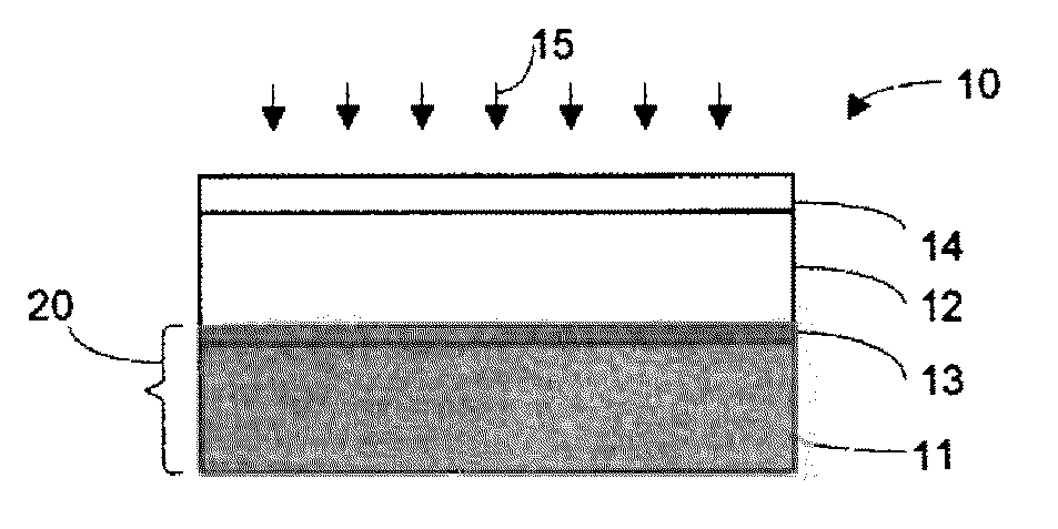
[0021]The present invention provides various methods to form Cu(In, Ga) (Se, S)2 absorber layers (CIGS) from electrodeposited precursors of the present invention. A precursor of the present invention may be formed as a stack having three layers. A first layer, which is copper poor, may be deposited over a base and a second layer, which is copper rich, deposited onto the first layer. A third layer including selenium is deposited onto the second layer before reacting the precursor to form the CIGS absorber layer. The first layer may include a Group IB-Group IIIA alloy or mixture of stacked films where the Group IB material is preferably Cu and the Group IIIA material is at least one of In and Ga. Such films may include (Cu-In), (Cu-Ga) and (Cu-In-Ga) alloy films or mixture such films. Alternatively, the first layer may include a mixture of stacked single element films, i.e., Cu, In, Ga films, or a mixture of such single element films and (Cu-In), (Cu-Ga) and (Cu-In-Ga) alloy films. Th...


PUM

PropertyMeasurementUnit
Fractionaaaaaaaaaa
Fractionaaaaaaaaaa

Abstract

The present invention provides a method and precursor structure to form a solar cell absorber layer. The method includes electrodepositing a first layer including a film stack including at least a first film comprising copper, a second film comprising indium and a third film comprising gallium, wherein the first layer includes a first amount of copper, electrodepositing a second layer onto the first layer, the second layer including at least one of a second copper-indium-gallium-ternary alloy film, a copper-indium binary alloy film, a copper-gallium binary alloy film and a copper-selenium binary alloy film, wherein the second layer includes a second amount of copper, which is higher than the first amount of copper, and electrodepositing a third layer onto the second layer, the third layer including selenium; and reacting the precursor stack to form an absorber layer on the base.

Description

CROSS REFERENCES TO RELATED APPLICATIONS[0001]This application is a Continuation-in-Part of U.S. patent application Ser. No. 12 / 123,372, filed May 19, 2008, entitled “ELECTROPLATING METHODS AND CHEMISTRIES FOR DEPOSITION OF GROUP IIIB-GROUP VIA THIN FILMS” (SP-050), and this application is a Continuation in Part of U.S. patent application Ser. No. 12 / 371,546 filed Feb. 13, 2009 entitled “ELECTROPLATING METHODS AND CHEMISTRIES FOR DEPOSITION OF COPPER-INDIUM-GALLIUM CONTAINING THIN FILMS” (SP-051), which claims priority to U.S. Provisional Application No. 61 / 150,721, filed Feb. 6, 2009, entitled “ELECTROPLATING METHODS AND CHEMISTRIES FOR DEPOSITION OF COPPER-INDIUM-GALLIUM CONTAINING THIN FILMS” (SP-051P), and this application is a Continuation in Part of U.S. patent application Ser. No. 12 / ______ filed on Dec. 18, 2009 entitled “ENHANCED PLATING CHEMISTRIES AND METHODS FOR PREPARATION OF GROUP IBIIIAVIA THIN FILM SOLAR ABSORBERS” (SP-098) and this application is a Continuation in P...

Claims


Application Information

Patent Timeline
IPC IPC(8): C25D7/12
CPCC25D3/38C25D5/10C25D3/58C25D3/54C25D5/611
Inventor AKSU, SERDARPINARBASI, MUSTAFA
Owner SOLOPOWER
Why Eureka
Try Eureka