Electrode of a light-emitting device of the OLED type

a light-emitting device and light-emitting device technology, which is applied in the manufacture of electric discharge tubes/lamps, instruments, and discharge tubes luminescnet screens, etc., can solve the problems of complex filter matrix production, reducing the useful surface area, and increasing the cost of microdisplay

Active Publication Date: 2010-06-10
COMMISSARIAT A LENERGIE ATOMIQUE ET AUX ENERGIES ALTERNATIVES
View PDF7 Cites 49 Cited by
  • Summary
  • Abstract
  • Description
  • Claims
  • Application Information

AI Technical Summary

Benefits of technology

[0009]An object of the present invention is to propose a solution for producing a light-emitting device of the OLED type which may emit light of different wavelengths from one pixel to the other, without complexifying the production of such a device, and at a cost less than that of methods of the prior art.

Problems solved by technology

But taking the dimensions of the pixels of these screens (a few microns) into account, the dimensions of alignment margins taken for the step for transferring the matrix of filters onto the cathode are equivalent to the dimensions of the pixels themselves, reducing the useful surface area and notably increasing the cost of the microdisplay.
But also in this case, an alignment during the photolithographic steps on the anodes and the transistors of the active matrix located under the organic layers is necessary, complexifying the production of this filter matrix.
Further, this solution is particularly aggressive for the organic layers which may be deteriorated.
However, producing such a stack of layers, with which the optical cavities may be tuned onto different colors from one pixel to the other, while retaining the same stack of organic layers for all the pixels and by modulating the thickness of these layers from one pixel to the other, is complex.
This approach therefore remains costly, notably for producing microdisplays.

Method used


Image

  • Electrode of a light-emitting device of the OLED type
  • Electrode of a light-emitting device of the OLED type
  • Electrode of a light-emitting device of the OLED type

Examples


first embodiment

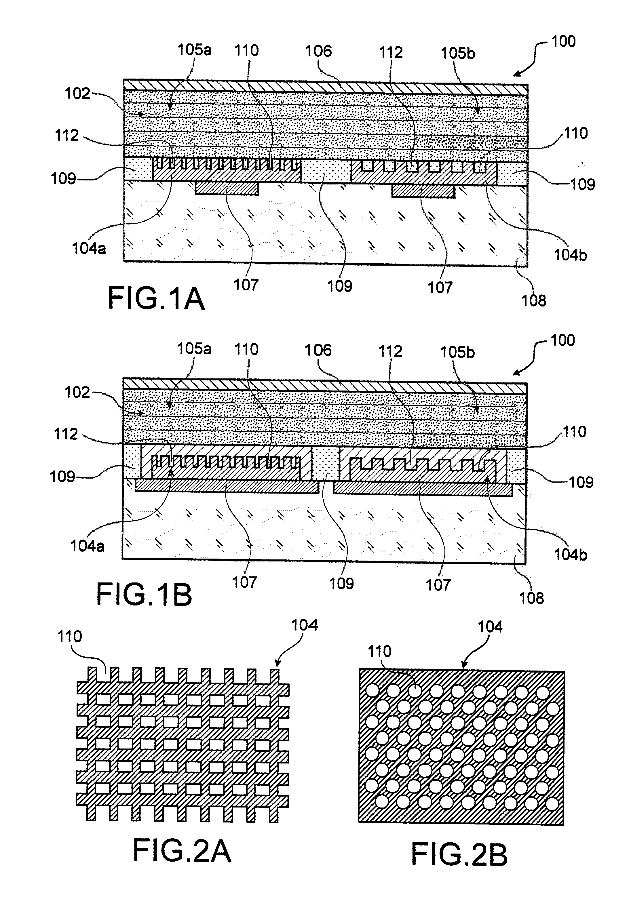
[0057]First of all reference will be made to FIG. 1A which illustrates a light-emitting device of the OLED type 100 according to a

[0058]The device 100 includes a stack of electroluminescent organic layers 102, positioned between a matrix of electrodes, here anodes, and an electrode 106, here a cathode, common to the entire device 100. In FIG. 1A, only two anodes 104a, 104b are illustrated. The device 100 also includes a substrate 108, for example based on silicon, comprising an addressing circuit formed in this first embodiment by an active matrix of transistors 107, or TFT matrix, in contact with the matrix of anodes 104a, 104b. In an alternative, this addressing circuit may also be achieved with integrated circuits. With each transistor 107, light emission from each pixel of the device 100 formed by one of the anodes 104a, 104a and a portion of the cathode 106 and of the stack of organic layers 102 located at the anode may be individually controlled by having a current flow betwee...

second embodiment

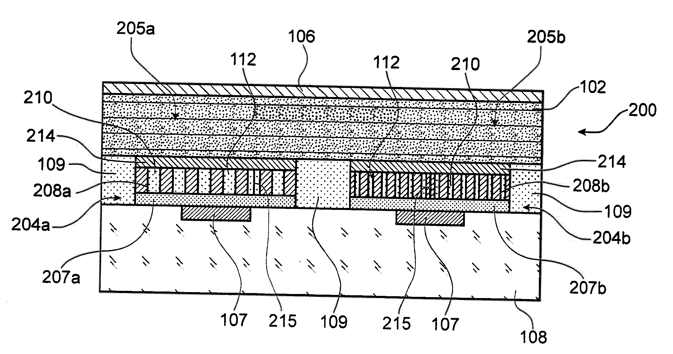
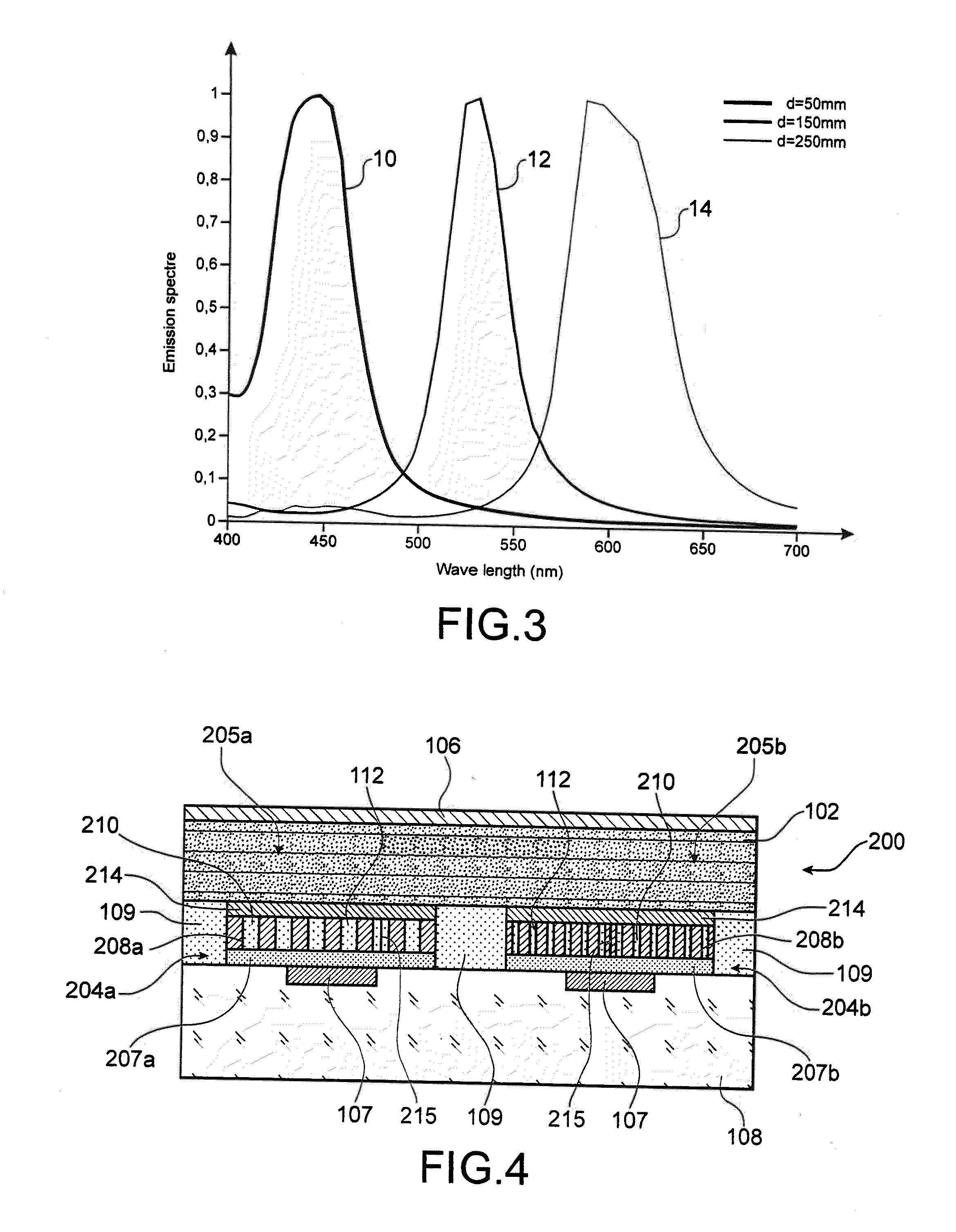
[0077]Reference will now be made to FIG. 4 which illustrates a light-emitting device of the OLED type 200 according to a

[0078]The device 200 includes the substrate 108 comprising the active matrix of transistors 107, the stack of electroluminescent organic layers 102, the filling material of refractive index n2, the insulating portion 109 and the cathode 106 for example similar to the corresponding components of the device 100 of FIG. 1A. The device 200 also includes a matrix of anodes positioned on the substrate 108. Two anodes 204a and 204b are illustrated in FIG. 4. Unlike the anodes 104a, 104b of FIG. 1A, the anodes 204a, 204b each include a layer 207a and 207b, respectively, positioned on the substrate 108, based on an electrically conducting material, for example similar to the material of the anodes 104 of FIG. 1A.

[0079]Each anode 204 also includes a layer 208a, 208b based on a material of refractive index n1 positioned on the conducting layer 207a, 207b. Patterns forming rec...


PUM


Abstract

An electrode of a light-emitting device of the OLED type adapted for forming with a second electrode, an optical cavity, including at least one layer based on a material of refraction index n1 including a structured face comprising a plurality of recesses filled with a material of refractive index n2 different from n1.

Description

TECHNICAL FIELD AND PRIOR ART[0001]The invention relates to a structured electrode of a light-emitting device of the OLED (Organic Light Emitting Diode) type and to an OLED device including such an electrode. The invention will be particularly suitable for making a device emitting light of several wavelengths, i.e. a multicolor display device, based on organic light-emitting layers used in a display or a screen of the OLED type, and notably in a microdisplay or the OLED type of centimetric dimensions.[0002]These microdisplays are small easily transportable screens and their viewing may be accomplished with enlarging optics. These devices are particularly suitable for producing viewing optics, for digital video or still cameras for example. These microdisplays are also suitable for operating in viewing glasses for example connected to a mobile video reader. A microdisplay should be inexpensive and have low electric consumption.[0003]A standard OLED type microdisplay includes a stack ...

Claims


Application Information

Patent Timeline
Patent Type & Authority Applications(United States)
IPC IPC(8): G09G5/00H01J1/62H01J9/00
CPCH01L27/3244H01L51/5265H01L51/5206H01L51/5203H10K59/30H10K59/12H10K50/813H10K50/81H10K50/852H10K50/858H10K50/805H10K50/85
Inventor DESIERES, YOHANGIDON, PIERREPOUPINET, LUDOVICMOUREY, BRUNO
Owner COMMISSARIAT A LENERGIE ATOMIQUE ET AUX ENERGIES ALTERNATIVES
Why Eureka
Try Eureka