Low voltage analog CMOS switch

a low-voltage analog, switch technology, applied in electronic switching, pulse technique, electric pulse generator details, etc., can solve the problems of increasing body effect related problems of conventional switch circuits based on mos transistors, etc., to increase resistance and leakage current, simple and cost-effective techniques

Active Publication Date: 2010-06-17
NUVOTON
View PDF15 Cites 15 Cited by
  • Summary
  • Abstract
  • Description
  • Claims
  • Application Information

AI Technical Summary

Benefits of technology

[0012]As noted above, conventional switch circuits based on MOS transistors often suffer from body effect related problems, such as increase resistance and leakage current. According to embodiments of the present invention, simple and cost-effective techniques are provided for a CMOS analog switch circuit suitable for low-voltage applications.
[0013]Embodiments of the present invention provide techniques for cost-effective analog switch circuit. In a specific set of embodiments, the invention provide techniques for applying adaptable body bias to one or more switch transistors in CMOS switch circuit to reduce resistance and leakage current in the switch circuit. In these embodiments, the bias circuit include native bias transistors and does not required additionally level-shifting circuitry, which can lead to chip area saving and cost reduction. In some embodiments, the body bias is adapted to be responsive to the terminal voltages of the CMOS switch to reduce threshold voltage increase caused by body effect in both directions of current flow. In other words, the effective threshold voltage is lowered in response to an input 
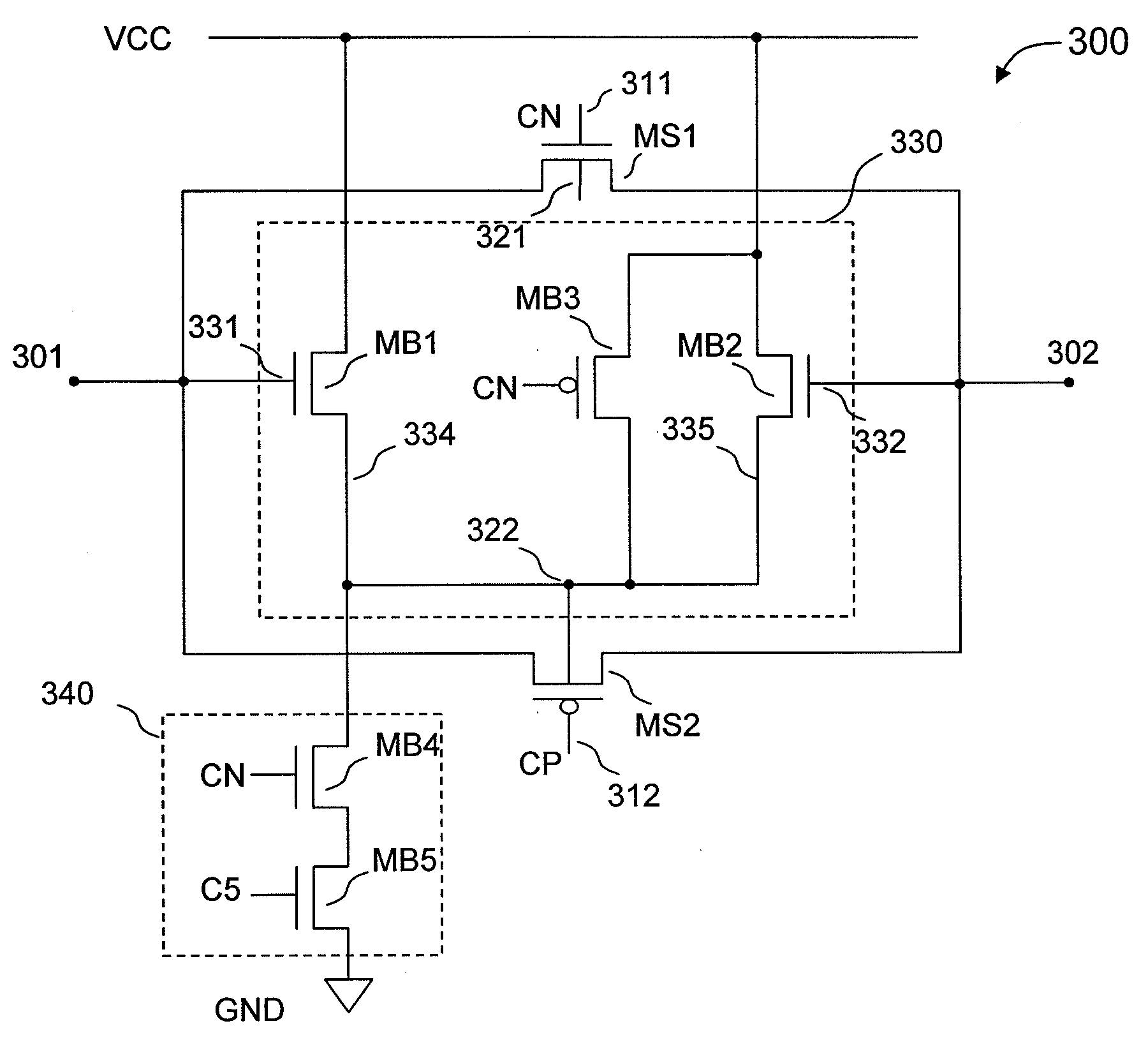
signal. As a result, the resistance of the switch circuit can be reduced. In other embodiments, the adaptable body bias can also be applied to an NMOS switch or a PMOS switch. Merely as an example, a bias circuit includes two native bias transistors having substantially 0V threshold voltages. The bias transistors have their source terminals coupled to the body terminal of a switch transistor, whereas their gate terminals are coupled, respectively, to the two terminals of the CMOS switch circuit. In other embodiments, the adaptable body bias can also be applied to an NMOS switch or a PMOS switch.
[0015]In a specific embodiment of the CMOS analog switch circuit described above, since the bias transistors are native transistors having substantially zero threshold voltages, the gate voltages of the bias transistors are substantially equal to the voltages at their respective source terminals which is coupled to the body terminal of the PMOS switch transistor. As a result, the bias circuit is configured to apply to the body terminal of the PMOS switch transistor the greater of the voltages of the first and second terminals of the CMOS analog switch circuit. Therefore, the effective source terminal is connected to the body terminal of the PMOS switch transistor, substantially independent of the direction or magnitude of current flow. As a result, the magnitude and variation of threshold voltage of the PMOS switch transistor is reduced, and the performance of the analog circuit employing such a CMOS switch can be improved.
[0020]Many benefits are achieved by way of the present invention over conventional techniques. For example, the present invention provides an easy to use designs that that are compatible with conventional integrated circuit design and fabrication process technologies. Embodiments of the invention provide techniques for cost-effective low voltage switches. In a specific set of embodiments, the invention provide techniques for applying adaptable body bias to one or more switch transistors in CMOS switch circuit to reduce the magnitude and variation in on-resistance in the switch circuit. In these embodiments, the bias circuit include native bias transistors and does not required additionally level-shifting circuitry, which can reduce complexity and lead to chip area saving and cost reduction. In some embodiments, the body bias is adapted to be responsive to the terminal voltages of the CMOS switch to reduce threshold voltage increase and variation caused by the so-called body effect. In other embodiments, the adaptable body bias can also be applied to an NMOS switch or a PMOS switch.
[0021]In some applications, embodiments of the invention can be used to reduce analog signal distortion in audio and video applications. In other applications, embodiments of the invention can be used to reduce incomplete settling on the sampling capacitors of analog to digital converters. In other embodiments, the techniques provided by the invention can also be used in switched capacitor circuit applications. It is understood that these techniques can be easily adopted for other applications requiring cost-effective analog switches, such as audio and video applications. Depending upon the embodiments, one or more of these benefits may be achieved. These and other benefits will be described in more detail throughout the present specification and more particularly below.

Problems solved by technology

As noted above, conventional switch circuits based on MOS transistors often suffer from body effect related problems, such as increase resistance and leakage current.

Method used


Image

  • Low voltage analog CMOS switch
  • Low voltage analog CMOS switch
  • Low voltage analog CMOS switch

Examples


Embodiment Construction

[0027]As discussed above, conventional analog switch circuits often suffer from various limitations. Some of the problems with these switches are that they have finite resistance when turned on and the resistance can vary non-linearly with the inputs signal, causing distortion. In addition, the finite on-resistance causes incomplete settling on the sampling capacitors of analog to digital converters. A major contributor to the large on-resistance of a CMOS switch in the application is the so-called transistor body effect, through which the transistor threshold voltage increases as the transistor source voltage to the body voltage increases. One technique to make the on-resistance smaller is to make the switches larger. However, larger switches consumes more integrated circuit dice area and introduces more leakage and charge injection when the switches are turned to the off position. Hence, there is a need to make a cost-effective low resistive switch without increasing switch area.

[...


PUM


Abstract

A CMOS analog switch circuit includes an NMOS switch transistor, a PMOS switch transistor, and a bias circuit. In an embodiment, the bias circuit includes a first and a second native bias transistors having their gate terminals coupled to a first and a second terminals of the CMOS switch circuit, respectively. The source terminals of the first and the second native bias transistors are coupled together and are also coupled to the body terminal of the PMOS switch transistor. In an configuration, the first and the second native bias transistors are characterized by substantially 0V threshold voltages, and the PMOS switch transistor is configured to exhibit a lower on-resistance in response to the greater of the voltages of the first terminal and the second terminal of the CMOS analog switch circuit.

Description

CROSS-REFERENCES TO RELATED APPLICATIONS[0001]NOT APPLICABLESTATEMENT AS TO RIGHTS TO INVENTIONS MADE UNDER FEDERALLY SPONSORED RESEARCH OR DEVELOPMENT[0002]NOT APPLICABLEREFERENCE TO A “SEQUENCE LISTING,” A TABLE, OR A COMPUTER PROGRAM LISTING APPENDIX SUBMITTED ON A COMPACT DISK.[0003]NOT APPLICABLEFIELD OF INVENTION[0004]The present invention relates generally to electronic circuit techniques. More specifically, embodiments of the present invention relate to techniques for cost effective low-voltage analog switch circuitry. Merely by way of example, embodiments of the invention have been applied to low-voltage analog CMOS switch circuit. But it would be recognized that the invention has a much broader range of applicability. For example, embodiments of the present invention can be applied in various low-voltage analog devices, including voice and audio band products.BACKGROUND OF THE INVENTION[0005]Voice and audio band applications often include selectable paths for selecting dif...

Claims


Application Information

Patent Timeline
Patent Type & Authority Applications(United States)
IPC IPC(8): H03K17/687
CPCH03K17/063H03K2217/0018H03K17/302
Inventor HOLZMANN, PETER
Owner NUVOTON
Why Eureka
Try Eureka