Semiconductor device

a technology of semiconductor devices and pin terminals, which is applied in the direction of printed circuit manufacturing, printed circuit construction, electrical apparatus construction details, etc., can solve the problems of reducing productivity, semiconductor devices being reduced in size and cost, and difficult to insert pin terminals into throughholes in printed boards, so as to facilitate mounting, facilitate alignment of pin terminals, and facilitate the effect of reducing size and cost of semiconductor devices

Inactive Publication Date: 2010-06-17
MITSUBISHI ELECTRIC CORP
View PDF0 Cites 59 Cited by
  • Summary
  • Abstract
  • Description
  • Claims
  • Application Information

AI Technical Summary

Benefits of technology

[0008]The present invention has been made to solve the above problems. It is, therefore, an object of the present invention to provide a semiconductor device with pin terminals and having a construction that facilitates the alignment of these pin terminals with throughholes in the substrate on which the semiconductor device is mounted and thereby facilitates the mounting, and that allows the semiconductor device to be reduced in size and cost.

Problems solved by technology

When mounting a modularized semiconductor device having many pin terminals of equal length to a printed board, it has sometimes been found difficult to insert these pin terminals into throughholes in the printed board.
As described above, when mounting a semiconductor device with many pin terminals of equal length to a substrate, it is difficult to align these pin terminals with throughholes in the substrate, resulting in reduced productivity.
However, the use of guide pins prevents the semiconductor device from being reduced in size and cost.

Method used


Image

  • Semiconductor device
  • Semiconductor device
  • Semiconductor device

Examples


embodiment

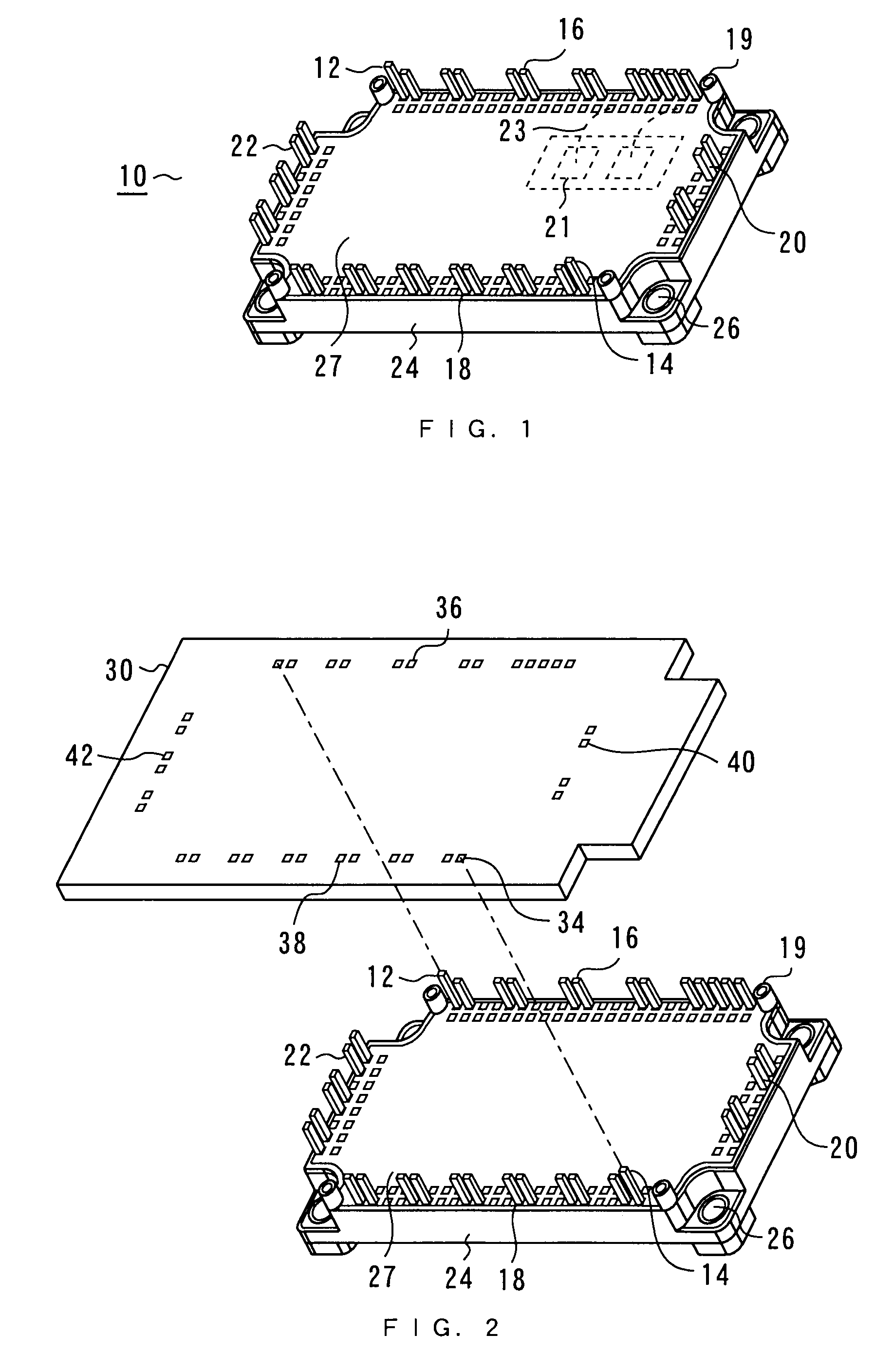
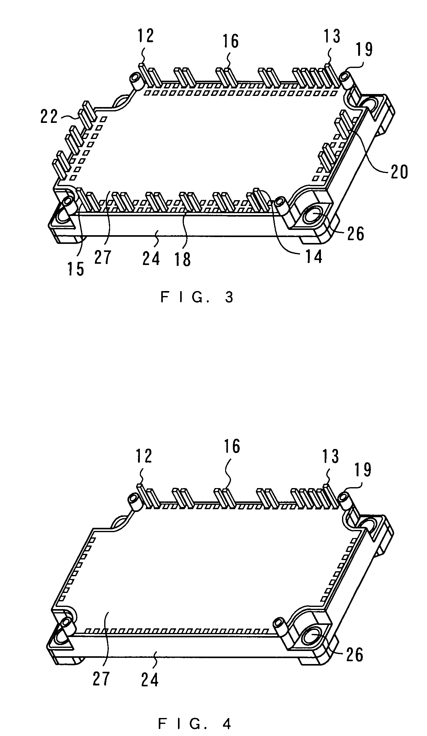
[0017]An embodiment of the present invention will be described with reference to FIGS. 1 to 6. It should be noted that like numerals represent like materials or like or corresponding components, and these materials and components may be described only once.

[0018]FIG. 1 is a perspective view of a semiconductor device 10 of the present embodiment. The semiconductor device 10 includes a boxy terminal case 24 of, e.g., resin in which semiconductor elements and pin terminals (described below) can be mounted. According to the present embodiment, the terminal case 24 contains a plurality of semiconductor elements 21 and a cover 27 which covers the elements 21. These semiconductor elements 21 are not externally visible and are shown in dashed line for convenience of illustration. The semiconductor elements 21 of the present embodiment are typically, but not limited to, IGBTs and their control circuits.

[0019]Each semiconductor element 21 is connected to a respective pin terminal 16 by a wire...


PUM


Abstract

A semiconductor device includes a terminal case containing a semiconductor element, a plurality of pin terminals of equal length mounted in the terminal case and electrically connected to the semiconductor element, the plurality of pin terminals projecting outward from a predetermined surface of the terminal case in the same direction, and at least one protruding pin terminal mounted in the terminal case and projecting outward from the predetermined surface of the terminal case in the same direction farther than the plurality of pin terminals.

Description

BACKGROUND OF THE INVENTION[0001]1. Field of the Invention[0002]The present invention relates to a semiconductor device with pin terminals for insertion into throughholes in a substrate.[0003]2. Background Art[0004]There is a practice of packaging a plurality of semiconductor elements in a case with pin terminals, forming a modularized semiconductor device. This semiconductor device is mounted on a printed board by inserting the pin terminals of its case into throughholes in the printed board. These pin terminals are then soldered to the printed board to secure the semiconductor device to the board.[0005]Examples of such modularized semiconductor devices with pin terminals include power modules, and it is common to mount these modules on a printed board by the method described above. For example, power modules with pin terminals containing an IGBT (Insulated Gate Bipolar Transistor), an inverter, or a converter are often mounted on a printed board by inserting the pin terminals into...

Claims


Application Information

Patent Timeline
Patent Type & Authority Applications(United States)
IPC IPC(8): H05K1/02
CPCH01L23/055H05K3/308H05K2201/10689H05K2201/10863H01L2924/0002H01L2924/00
Inventor MATSUMOTO, MASAFUMIMIYAZAKI, YUJI
Owner MITSUBISHI ELECTRIC CORP
Why Eureka
Try Eureka