Method of cutting laminate with laser and laminate

a laser and laminate technology, applied in the field of cutting laminates and laminates, can solve the problems of affecting the quality of laminates, so as to achieve the effect of reducing size and cost, and efficient production of high-quality devices

Inactive Publication Date: 2005-12-08
FUJITSU LTD
View PDF11 Cites 10 Cited by
  • Summary
  • Abstract
  • Description
  • Claims
  • Application Information

AI Technical Summary

Benefits of technology

[0015] The laminate comprising a plurality of substrates of different materials can be cut at a time by the irradiation of a single laser and,

Problems solved by technology

In fabricating a device having a fine mechanism such as a MEMS device, however, an attempt to separate the laminate into individual devices using the wheel containing diamond abrasive grains poses the problem that the contact between the wheel and the laminate at the time of cutting operation causes the laminate to vibrate and often damages the fine mechanism of the device.
In the cutting method using the laser, however, the material is required to absorb the laser light, and therefore the combinations of the lasers and the materials to be cut are limited.
In the case where the laminate includ

Method used


Image

  • Method of cutting laminate with laser and laminate
  • Method of cutting laminate with laser and laminate
  • Method of cutting laminate with laser and laminate

Examples


Embodiment Construction

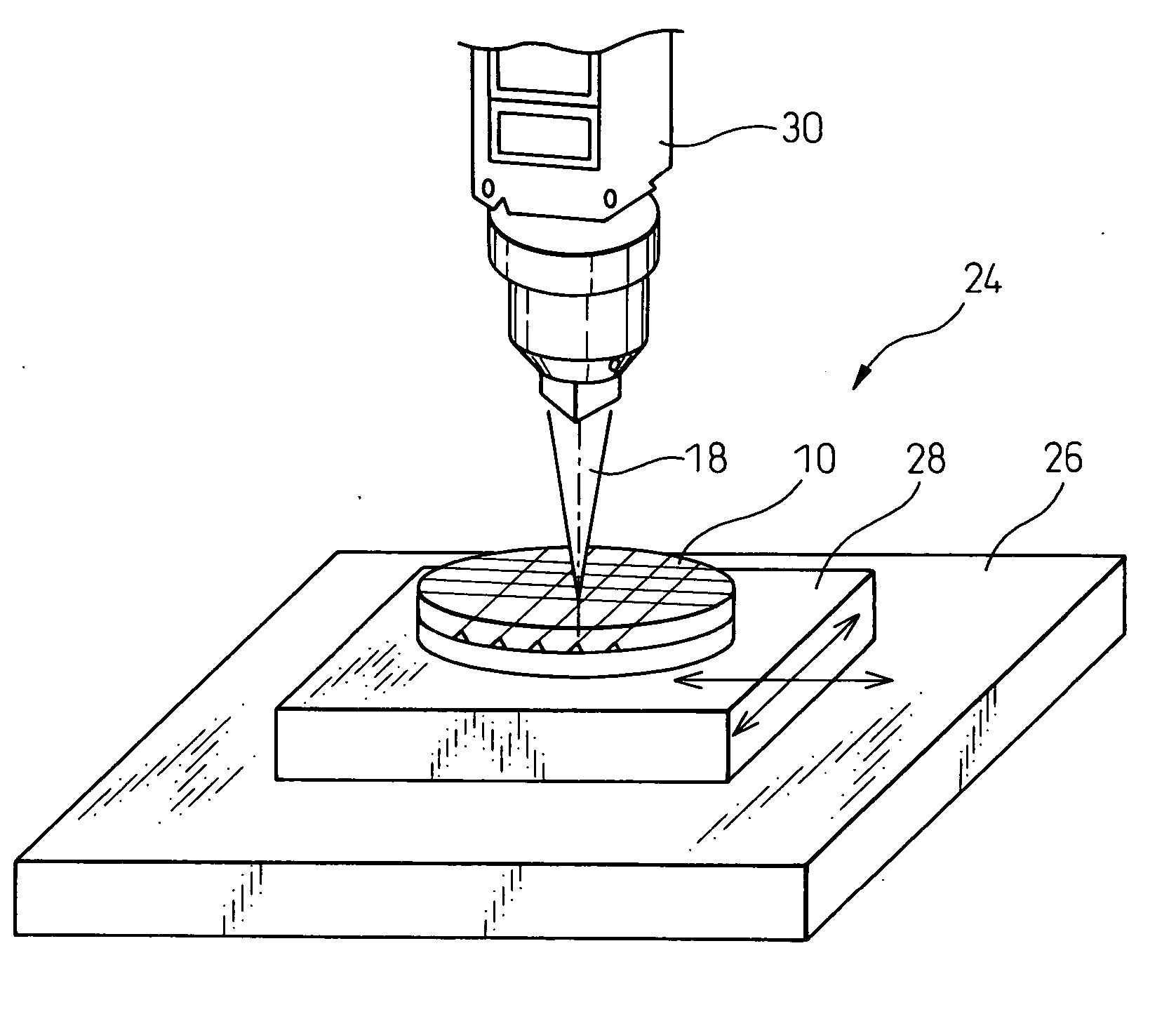
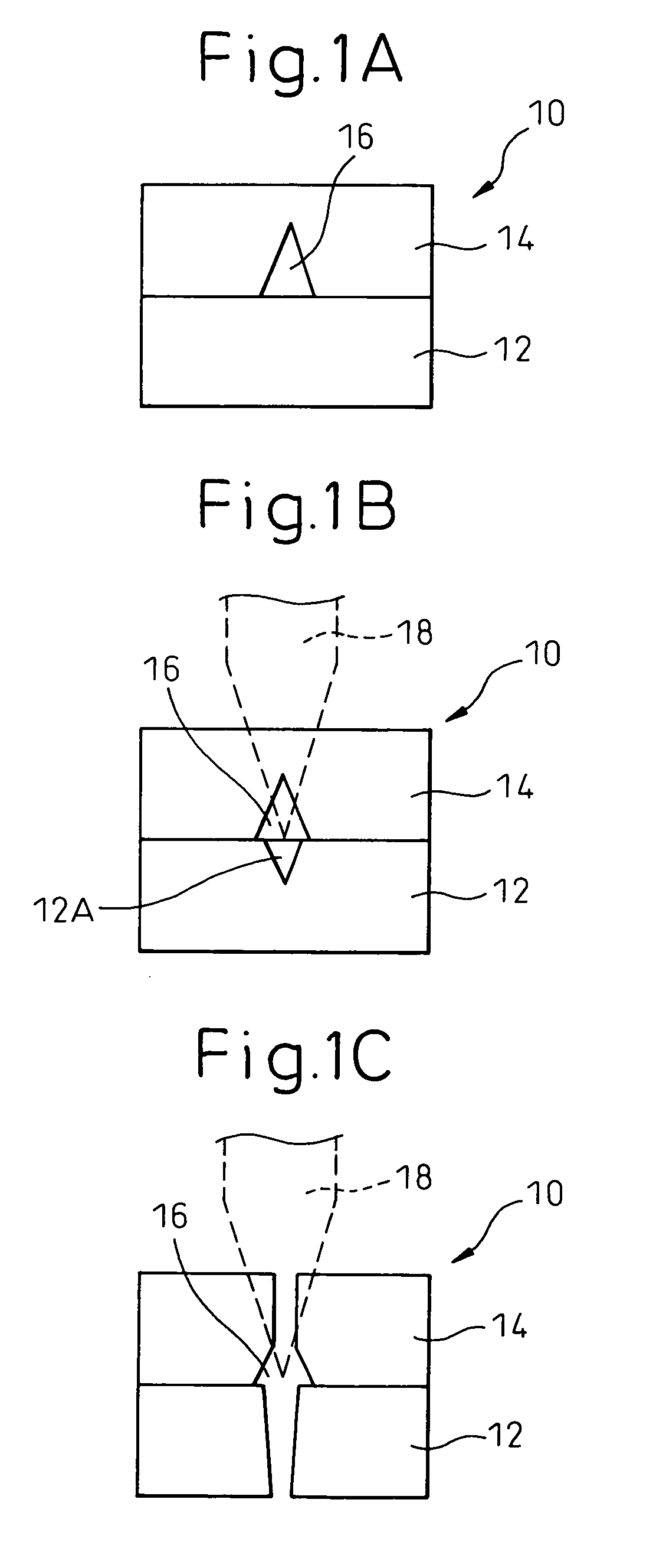
[0026] The preferred embodiments of the present invention are described below with reference to the drawings. FIGS. 1A to 1C are diagrams showing a method of cutting a laminate according to the present invention.

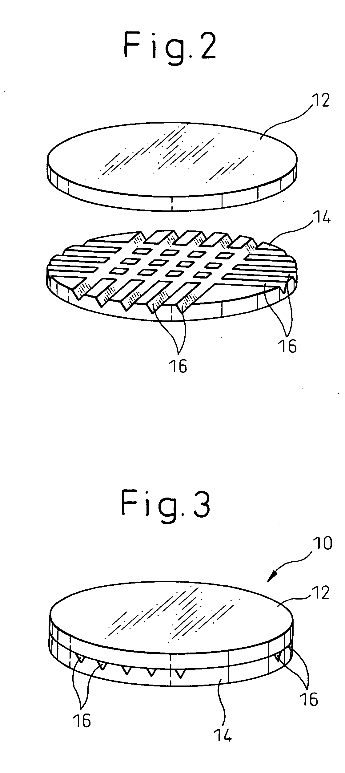
[0027] In FIG. 1A, a laminate 10 comprising a first substrate 12 and a second substrate 14 is prepared. The second substrate 14 has a groove 16. An explanation is made below with reference to an example in which a plurality of MEMS devices are fabricated, but the present invention is not limited to this example. The laminate 10 has circuits and fine mechanisms formed therein corresponding to a plurality of MEMS devices, and cut into individual MEMS devices separated from each other. The groove 16 is formed along a cutting line for separating the laminate into MEMS devices.

[0028] The first substrate 12 is formed of a semiconductor, i.e. constitutes a silicon wafer formed with circuits and fine mechanisms. The second substrate 14 is formed of pyrex glass, and the groove 16 i...


PUM

PropertyMeasurementUnit
Shapeaaaaaaaaaa

Abstract

A device such as an MEMS device is fabricated by cutting a laminate of a semiconductor substrate and a glass substrate. Grooves are formed in the glass substrate, and the semiconductor substrate and the glass substrate are laminated together such that the groove faces the semiconductor substrate. The laminated substrates are irradiated with a laser along the groove from the side of the glass substrate. In this way, the laminate is cut into elements.

Description

BACKGROUND OF THE INVENTION [0001] 1. Field of the Invention [0002] The present invention relates to a method of cutting a laminate and a laminate and, in particular, it relates to a method of cutting a laminate formed of substrates of different types of materials. [0003] 2. Description of the Related Art [0004] A device comprising a laminate including a plurality of substrates of different types of materials has recently been developed. Highly technical devices such as MEMS devices are configured as a laminate of a substrate formed of silicon, and a substrate of lithium tantalate (LiTaO3), sapphire, or heat-resistant glass, etc, superposed together. In fabricating such a device, the laminate composed of a plurality of substrates of different types of materials is cut into separate devices (chips). [0005] In a conventional method, a semiconductor wafer is cut into separate semiconductor chips by rotating a wheel containing diamond abrasive grains at high speed. The wheel containing ...

Claims


Application Information

Patent Timeline
IPC IPC(8): B23K26/40B31B50/25B32B17/06B81C1/00B81C99/00C03B33/00C03B33/07C03B33/09H01L21/78
CPCB23K26/0054B23K26/4075B23K2201/40B32B17/06B81C1/00888Y10T156/1052C03B33/091H01L21/78B23K26/0057B23K26/0063Y10T156/1064C03B33/07B23K26/40B23K26/50B23K26/53B23K26/57B23K2101/40B23K2103/50Y10T83/0304Y10T83/0333Y10T83/0341
Inventor FURUI, TOSHIKAZUMATSUSHITA, NAOHISA
Owner FUJITSU LTD
Why Eureka
Try Eureka