Resonator and dielectric filter

a dielectric filter and resonator technology, applied in the field of resonators and dielectric filters, can solve the problems of inability to miniaturize filters, and inability to obtain desired filter characteristics in some cases, so as to reduce size and cost, suppress loss, and high accuracy

Inactive Publication Date: 2007-07-17
SONY CORP
View PDF15 Cites 11 Cited by
  • Summary
  • Abstract
  • Description
  • Claims
  • Application Information

AI Technical Summary

Benefits of technology

[0009]It is an object of the present invention to provide a resonator and a dielectric filter which can be reduced in size and costs and have desired characteristics with a high accuracy and a suppressed loss.
[0013]According to the present invention, one pair of resonant electrodes is formed in a loop shape or a spiral shape in a substrate stacking direction symmetrically to each other. This allows a longitudinal space in substrate to be reduced, thereby miniaturizing the resonator and the dielectric filter. The first capacitor having one end connected to the grounding conductor layer and the other end connected to the signal input terminal or the resonant electrode whose open-end side is used as the signal input terminal, and the second capacitor having one end connected to the grounding conductor layer and the other end connected to the signal output terminal or the resonant electrode whose open-end side is used as the signal output terminal, are provided so that the resonant electrode may be further reduced, thereby reducing the instrument in size. Further, the third capacitor having one end connected to the signal input terminal or the resonant electrode whose open-end side is used as the signal input terminal and the other end connected to the signal output terminal or the resonant electrode whose open-end side is used as the signal output terminal is provided. This allows a trapped frequency to be adjusted, by adjusting static capacitance of the third capacitor. Additionally, using tantalum oxide as dielectric material causes an area occupied by the capacitor on the substrate to be reduced, thereby reducing the instrument in size. Since the layer of conductive material arranged between the grounding conductor layer and the resonant-pattern conductor layer includes a slot so that it may contain a region facing the resonant electrodes, the resonator or the dielectric filter having a desired characteristic may be obtained without receiving any influence from other signal pattern wiring line,

Problems solved by technology

However, in the case of, for example, a comb-line type filter by which one pair of conductor patterns each having a length that is one fourth a wavelength of a signal to be transmitted therethrough is coupled to each other electromagnetically, if the signal to be transmitted has a low frequency, the conductor patterns must be elongated, to make it impossible to miniaturize the filter.
Furthermore, if an instrument is miniaturized by configuring into a multi-layer structure such layers as filter layers designed as those of a distributed parameter circuit and pattern wiring line layers, behaviors of the filter are influenced by signal wiring line patterns etc, thus making it impossible to obtain desired filter characteristics in some cases.
For example, if a signal wiring line pattern is arranged between a grounding conductor layer and conductor patterns, a condition of electromagnetic coupling between one pair of parallel conductor patterns changes, thereby making it impossible to obtain desired filter characteristics in some cases.

Method used


Image

  • Resonator and dielectric filter
  • Resonator and dielectric filter
  • Resonator and dielectric filter

Examples


Embodiment Construction

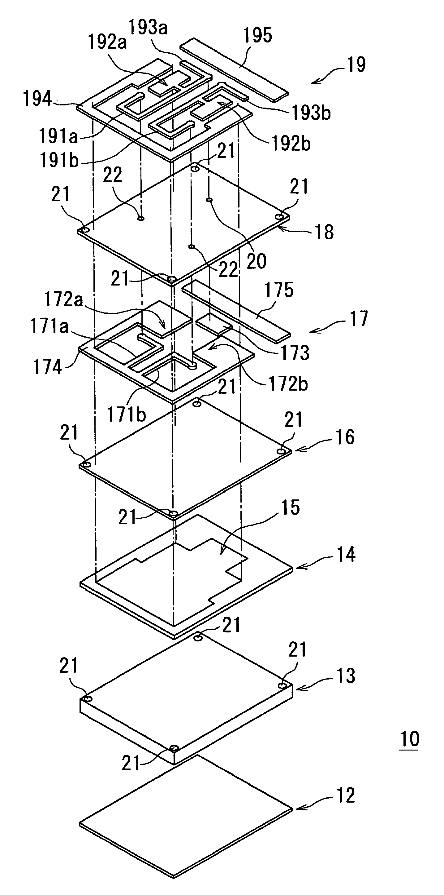
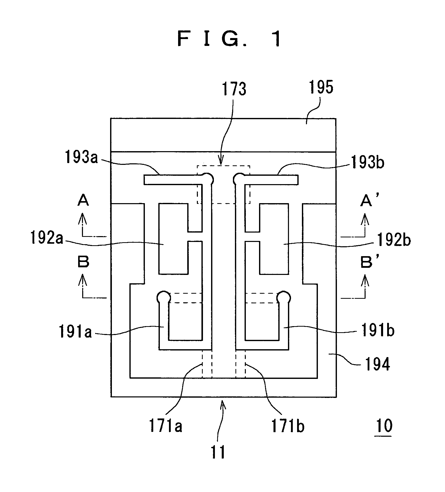
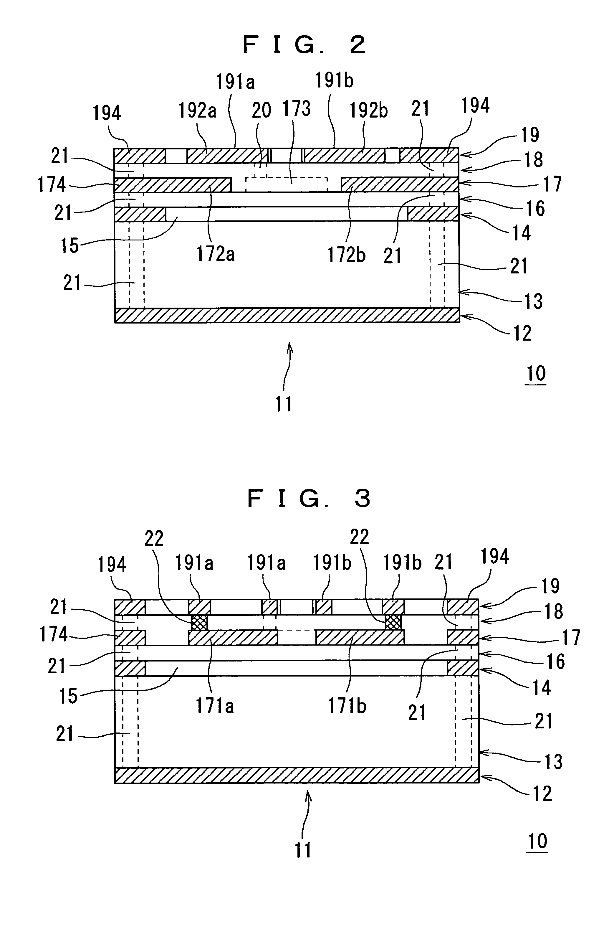
[0026]The following will describe embodiments of the present invention with reference to drawings. FIG. 1 is a plan view of a configuration of a dielectric filter 10. FIG. 2 is a cross-sectional view of the dielectric filter 10 taken along line A–A′ in FIG. 1. FIG. 3 is a cross-sectional view of the dielectric filter 10 taken along line B–B′ in FIG. 1. FIG. 4 is an exploded perspective view of the dielectric filter 10. FIGS. 1–4 show the dielectric filter 10 in a condition where one pair of resonant electrodes is formed symmetrically to each other in a spiral shape in a substrate stacking direction.

[0027]On a rear side of a stack substrate 11 in which multiple layers of dielectric material (hereinafter referred to as “dielectric layer”) and conductive material (hereinafter referred to as “conductor layer”) are stacked, a first conductor layer 12 is formed as a grounding conductor layer. On, for example, the right layer side of the stack substrate 11 opposite the first conductor laye...


PUM


Abstract

One pair of resonant electrodes is formed in a loop shape or a spiral shape in a substrate stacking direction symmetrically to each other. This allows a longitudinal space in substrate to be reduced. A first capacitor having an electrode connected to the grounding conductor layer, an electrode connected to an open-end side of the resonant electrode, and a dielectric layer is provided. A second capacitor having an electrode connected to the grounding conductor layer, an electrode connected to an open-end side of the resonant electrode, and a dielectric layer is also provided. This results in having a desired characteristic even if a length of the resonant electrode is short.

Description

BACKGROUND THE INVENTION[0001]1. Field of the Invention[0002]The present invention relates to a resonator and a dielectric filter.[0003]2. Description of the Related Art[0004]As a communication system using a high-frequency radio wave in a microwave-band or a millimeter-wave band as a carrier, for example, a telephone system such as a cellular phone or a wireless local area network (LAN) has become widely used, it has become possible to transmit and receive a variety of types of data easily and not through a repeater etc., at a variety of places both indoors and outdoors.[0005]An instrument used in such a communication system is provided with a filter element such as a low-pass filter (LPF), a high-pass filter (HPF), or band-pass filter (BPF). The filter element is designed so that it can be used in a distributed parameter circuit, not in a lumped parameter circuit, in order to process a signal in the high-frequency band. For example, a filter having a tri-plate structure is formed ...

Claims


Application Information

Patent Timeline
Patent Type & Authority Patents(United States)
IPC IPC(8): H01P1/203H01P1/205H01P7/08
CPCH01P1/20381H01P7/08H01P1/203
Inventor MUTO, AKIRA
Owner SONY CORP
Why Eureka
Try Eureka