Gas supply system for semiconductor manufacturing facilities

a technology for semiconductor manufacturing and gas supply system, which is applied in the direction of instruments, process and machine control, coatings, etc., can solve the problems of difficult to compact the gas supply system, many problems to be overcome, and complex equipment and systems, so as to achieve effective use and high responsiveness, and prevent the reduction of the sharpness of the interface between thin films. , the effect of high responsiveness

Active Publication Date: 2013-12-10
FUJIKIN INC
View PDF60 Cites 10 Cited by
  • Summary
  • Abstract
  • Description
  • Claims
  • Application Information

AI Technical Summary

Benefits of technology

[0026]In accordance with the present invention, the flow rate control of the main gas supply line L1 and the pressure control of the vent gas supply line L2 are performed using the pressure type flow-rate control system and the pressure control system having a configuration similar to this flow-rate control system, and, therefore, a difference in pressure between the gas supply lines L1 and L2 can be instantaneously adjusted and kept at zero by effectively using a high responsiveness inherent to the pressure type flow-rate control system and the pressure control system. As a result, the occurrence of a difference in pressure between both lines L1 and L2 is never caused when switching between source supply gases is performed, and, therefore, a transient flow phenomenon does not occur when a new source gas is supplied, and a so-called decrease in sharpness of the interface between thin films is prevented, and, as a result, a high-quality semiconductor product can be obtained.
[0027]Additionally, a pressure detector and a calculation control unit, which are components of the pressure type flow-rate control system and of the pressure control system, can be used completely and without being modified, and, unlike the conventional system, both of the lines L1 and L2 are not required to have a pressure regulator or a feedback control line FBL. Therefore, the equipment can be reduced in size and cost.

Problems solved by technology

However, many problems to be overcome still remain in the gas supply system of FIG. 10.
Therefore, the equipment and systems are complicated, and a large space is needed to mount the differential pressure detector DP, thus making it difficult to make the gas supply system compact.

Method used


Image

  • Gas supply system for semiconductor manufacturing facilities
  • Gas supply system for semiconductor manufacturing facilities
  • Gas supply system for semiconductor manufacturing facilities

Examples


Embodiment Construction

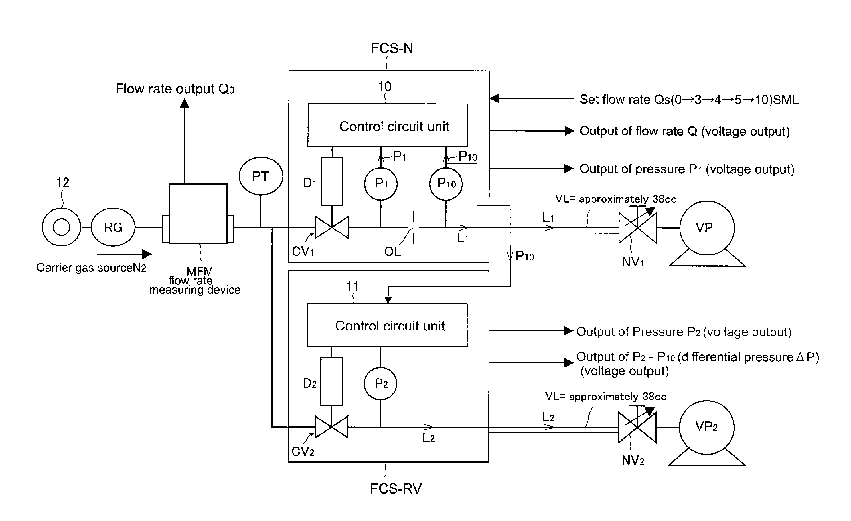
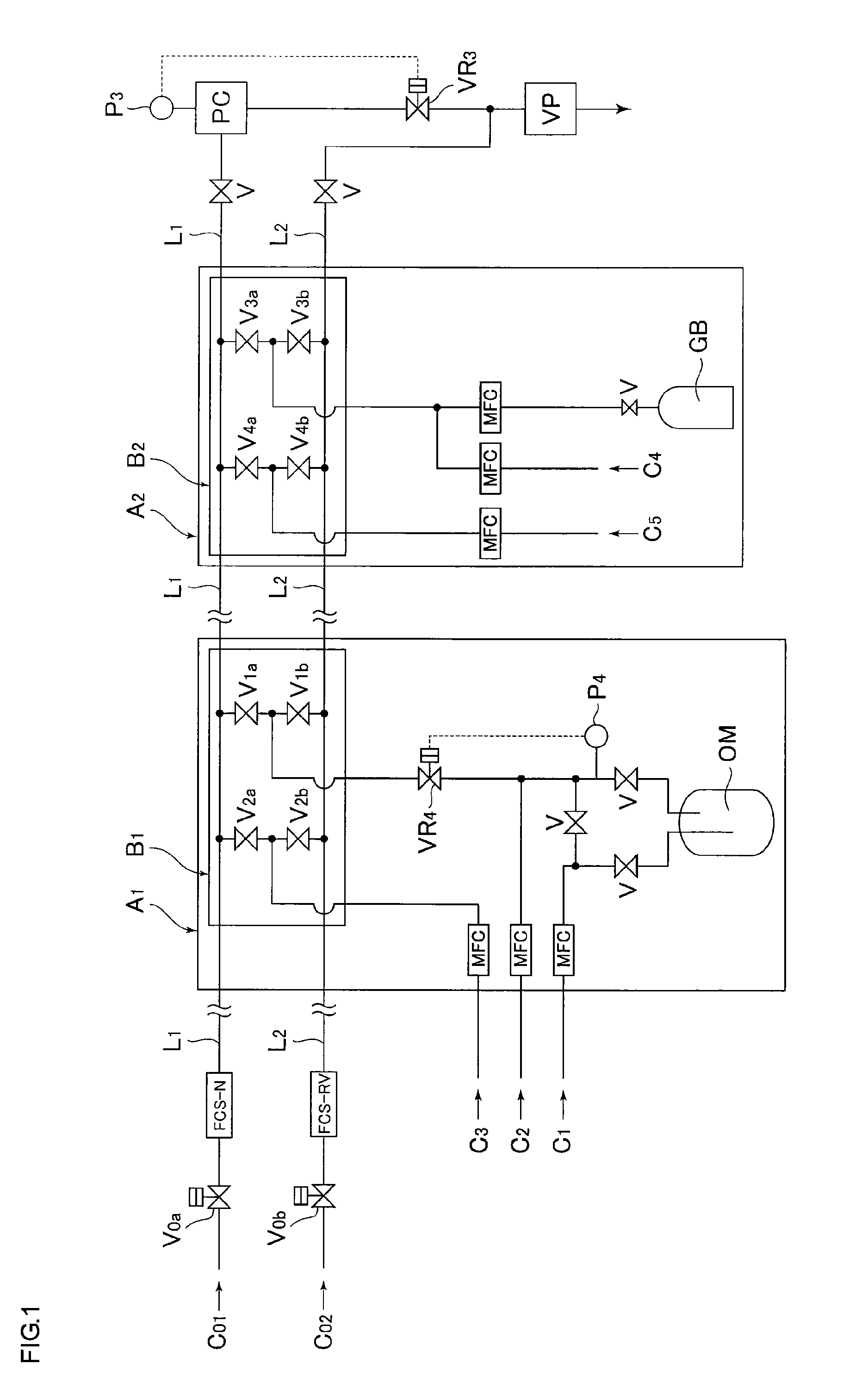
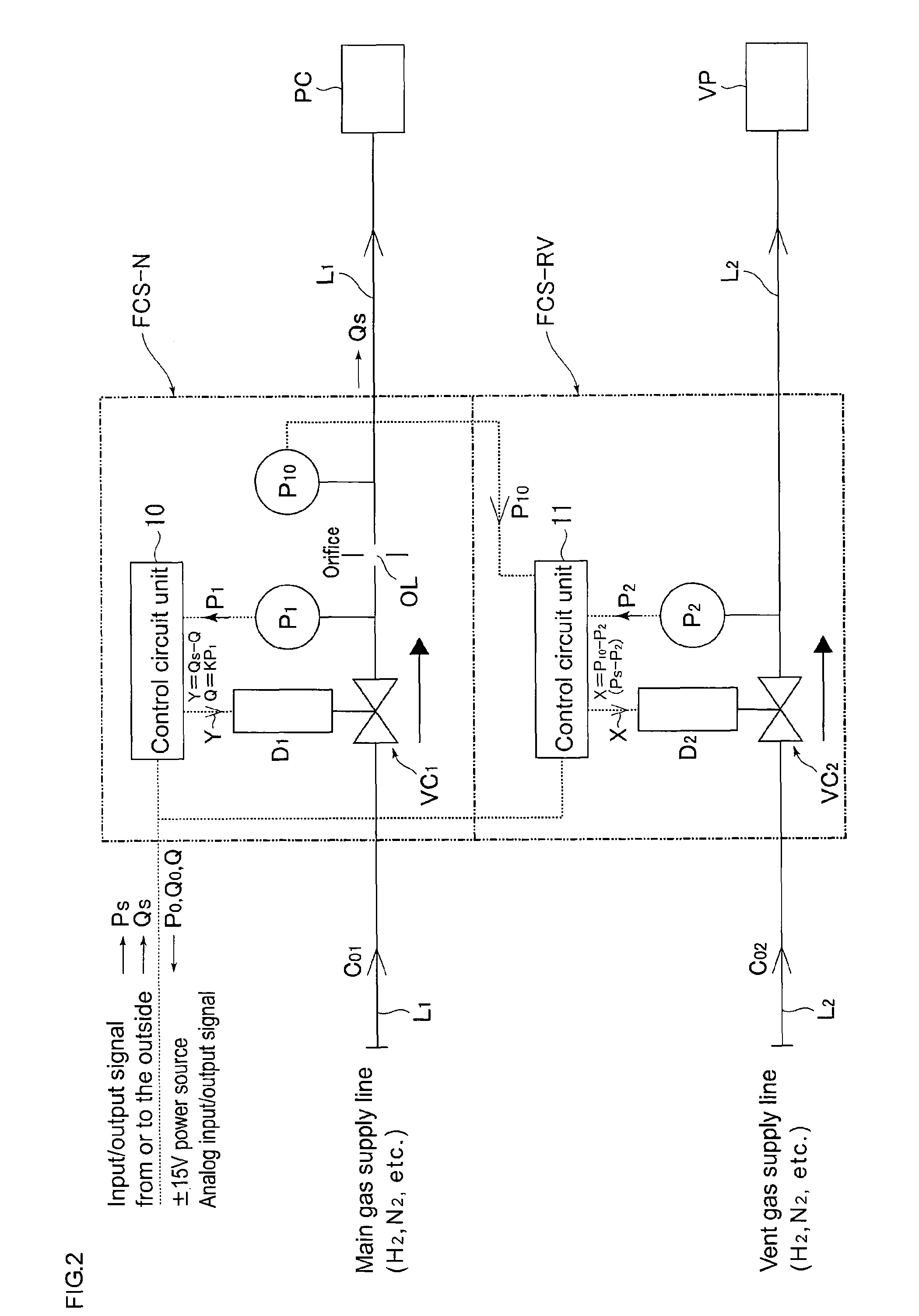
[0039]An embodiment of the present invention will be hereinafter described with reference to the drawings. FIG. 1 shows an embodiment of a gas supply system for semiconductor manufacturing facilities according to the present invention. In FIG. 1, FCS-N designates a pressure type flow-rate control system, FCS-RV designates a pressure control system, A1 designates a mechanism for supplying an organometallic source gas, A2 designates a mechanism for supplying another source gas, L1 designates a main gas supply line, and L2 designates a vent gas supply line. The other configuration members are the same as those of the conventional gas supply system shown in FIG. 10 and, therefore, a description of the same members is omitted here and the same reference characters are used to designate like parts.

[0040]In other words, the present invention differs from the conventional gas supply equipment mainly in the fact that, in the present invention, the mass-flow controllers MFC1 and MFC2, the dif...


PUM

PropertyMeasurementUnit
exhaust pressureaaaaaaaaaa
diameteraaaaaaaaaa

Abstract

A gas supply system includes a main gas supply line; a vent gas supply line; a plurality of gas supply mechanisms disposed in middle of both gas supply lines; a pressure type flow-rate control system disposed on an inlet side of the main gas supply line so a flow of carrier gas is supplied to the main gas supply line; a pressure control system disposed on an inlet side of the vent gas supply line, a carrier gas having a predetermined pressure is supplied to the vent gas supply line while the pressure control system performs a pressure adjustment, a gas pressure of the main gas supply line detected downstream from an orifice of the pressure type flow-rate control system and a gas pressure of the vent gas supply line are compared, and the gas pressure of the vent gas supply line is adjusted so a difference therebetween becomes zero.

Description

[0001]This is a National Phase Application in the United States of International Patent Application No. PCT / JP2008 / 001920 filed Jul. 17, 2008, which claims priority on Japanese Patent Application No. 2007-246558, filed Sep. 25, 2007. The entire disclosures of the above patent applications are hereby incorporated by reference.TECHNICAL FIELD OF THE INVENTION[0002]This invention relates to a gas supply system for semiconductor manufacturing facilities that is mainly used as a gas supply system for a metal organic chemical vapor deposition system.BACKGROUND ART OF THE INVENTION[0003]In a semiconductor having a thin-film-laminated structure produced by a so-called “metal organic chemical vapor deposition method” (hereinafter, referred to simply as an “MOCVD method”), the improvement of sharpness in the interface between thin films of the laminated structure, formed by epitaxial growth, is an indispensable requirement to improve the quality of the semiconductor. In other words, in order ...

Claims


Application Information

Patent Timeline
Patent Type & Authority Patents(United States)
IPC IPC(8): C23C16/52C23F1/00H01L21/306C23C16/06C23C16/22
CPCC23C16/455C23C16/45561C23C16/52G05D7/0664
Inventor NISHINO, KOUJIDOHI, RYOUSUKENAGASE, MASAAKIHIRATA, KAORUSUGITA, KATSUYUKIIKEDA, NOBUKAZU
Owner FUJIKIN INC
Why Eureka
Try Eureka