Sputtering apparatus and method of manufacturing electronic device

a technology of sputtering apparatus and electronic device, which is applied in the direction of vacuum evaporation coating, electrolysis components, coatings, etc., can solve the problems of electrical power not being stably supplied to the cathode, the line extending from the connection terminal is often a load and twist, and the cathode cannot be connected stably

Inactive Publication Date: 2010-06-24
CANON ANELVA CORP
View PDF1 Cites 2 Cited by
  • Summary
  • Abstract
  • Description
  • Claims
  • Application Information

AI Technical Summary

Benefits of technology

[0013]It is an object of the present invention to provide a sputtering apparatus which can solve at least one of the problems of the related art. An example of that object is to provide a sputtering apparatus which can adjust the angle of a target with respect to a substrate.
[0020]According to the arrangement of the present invention, instability of power supply can be eliminated, and the angle of a target with respect to a substrate can be adjusted.

Problems solved by technology

However, in the sputtering apparatus described in Japanese Patent Laid-Open No. 2000-265264, the connection terminals 75 and lines extending from them often suffer a load and twist due to the rotary motion of the cathode rotary member 70.
Owing to such load and twist, electric power cannot be stably supplied to the cathode 60.
From the aforementioned points, for the sputtering apparatus described in Japanese Patent Laid-Open No. 2000-265264, it is difficult to adjust the angle of the cathode or target with respect to a substrate.

Method used


Image

  • Sputtering apparatus and method of manufacturing electronic device
  • Sputtering apparatus and method of manufacturing electronic device
  • Sputtering apparatus and method of manufacturing electronic device

Examples


Embodiment Construction

[0029]Embodiments of the present invention will be described hereinafter with reference to the drawings.

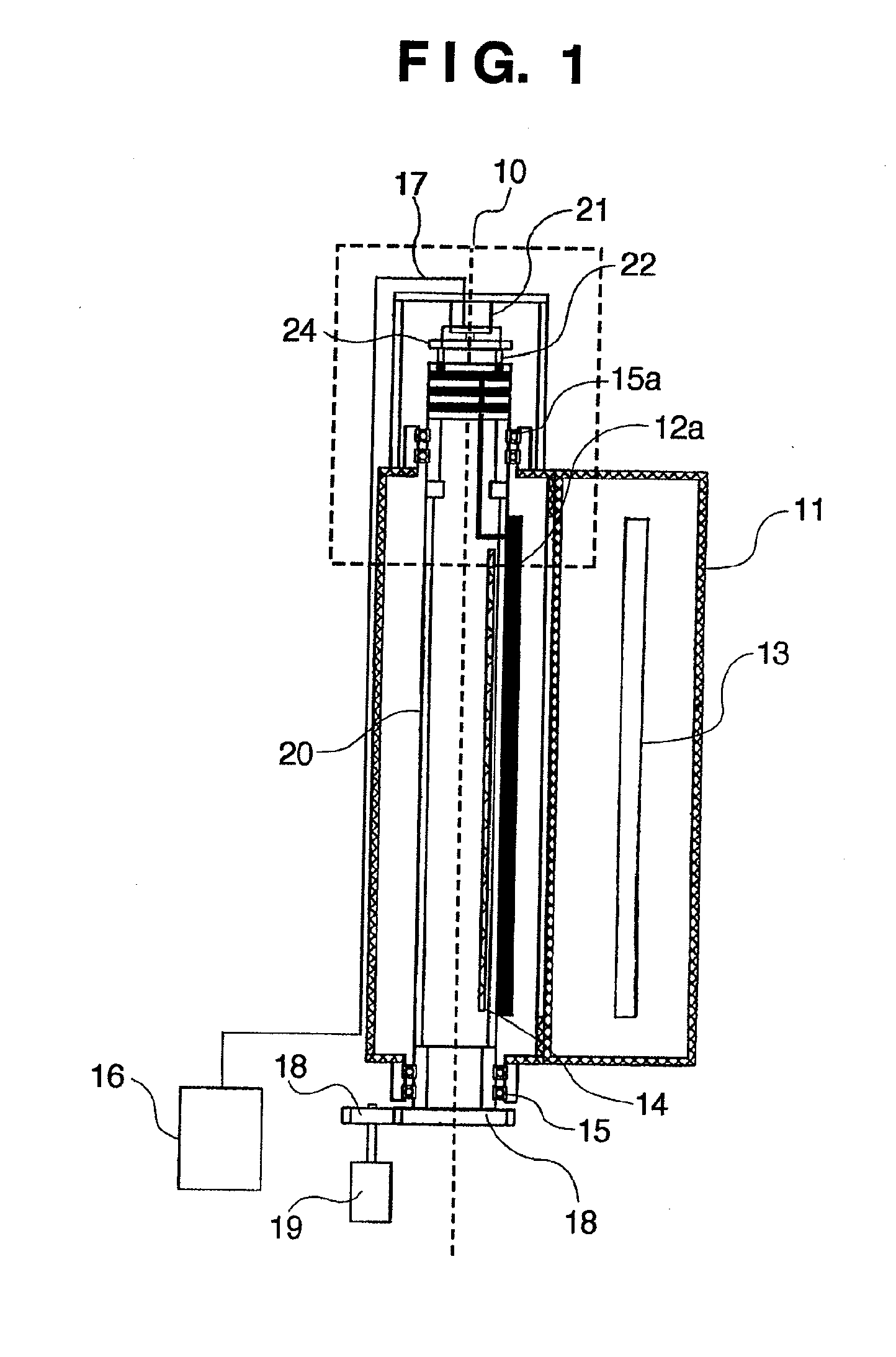
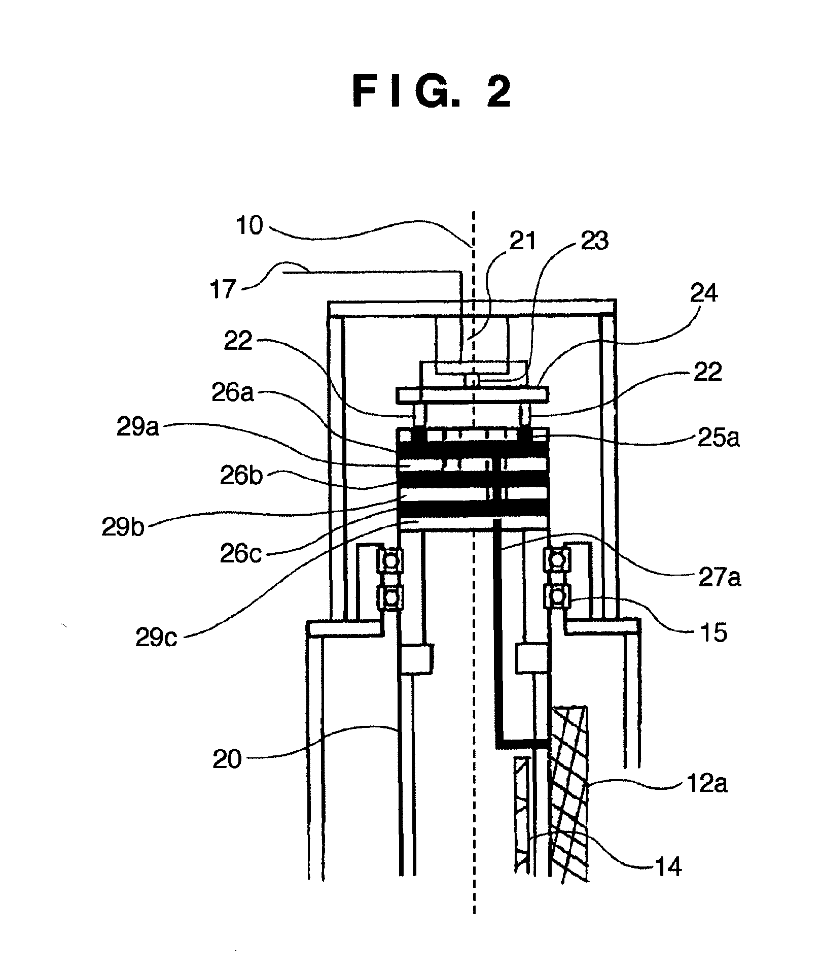
[0030]FIG. 1 is a sectional view of a sputtering apparatus according to an embodiment of the present invention. FIG. 2 is an enlarged view of the sputtering apparatus in a region bounded by the dotted line in FIG. 1. FIG. 3 is a plan view of a rotary member 20 viewed from a direction along an axis of rotation 10 of the rotary member 20.

[0031]In this embodiment, the sputtering apparatus has a chamber 11, rotatable rotary member 20, and substrate holder 13 which holds a substrate (not shown). The rotary member 20 has a nearly regular triangular prism shape, and a central axis of the triangular prism serves as an axis of rotation 10 of rotation. Three side surfaces along the axis of rotation 10 of this rotary member 20 respectively serve as cathodes. Targets 12a, 12b, and 12c as materials to be sputtered are detachably attached to these side surfaces.

[0032]The shape of the rotary mem...


PUM

PropertyMeasurementUnit
rotation angleaaaaaaaaaa
rotationaaaaaaaaaa
electric poweraaaaaaaaaa

Abstract

A sputtering apparatus includes a rotatable rotary member to which a target is attached, connection terminals, and feeding terminals. The connection terminals are arranged on the end portion of the rotary member in a direction along the axis of rotation of the rotary member, and are electrically connected to the target. The feeding terminals supply electric power to the target via the connection terminals. When the rotary member is rotated while the feeding terminals are in contact with the end portion of the rotary member, the electrical connection or insulation state between the feeding terminals and connection terminals is switched.

Description

BACKGROUND OF THE INVENTION[0001]1. Field of the Invention[0002]The present invention relates to a sputtering apparatus, which is applicable to deposition processing, surface treatment, and the like, and a method of manufacturing an electronic device.[0003]2. Description of the Related Art[0004]FIG. 6 is a sectional view showing the internal structure of a sputtering apparatus which is used to sputter a target, and is described in Japanese Patent Laid-Open No. 2000-265264. A sputtering apparatus shown in FIG. 6 has a rotatable cathode rotary member 70. Note that FIG. 6 shows a section perpendicular to the axis of rotation of the cathode rotary member 70. Cathodes 60 arranged on the side surfaces of the cathode rotary member 70 have a plurality of targets 72.[0005]The cathode rotary member 70 has four side surfaces in its direction of rotation, and the cathodes 60 are arranged on the four side surfaces of the cathode rotary member 70. Each cathode 60 has a feeding connection terminal...

Claims


Application Information

Patent Timeline
Patent Type & Authority Applications(United States)
IPC IPC(8): C23C14/34
CPCC23C14/3407C23C14/352H01J37/34H01J37/3266H01J37/32568
Inventor TAKIGUCHI, SHOJIUENO, HIDEKITAKANO, HIROSHI
Owner CANON ANELVA CORP
Why Eureka
Try Eureka