Butterfly-shaped semiconductor laser automatic coupling packaging device

A technology for automatic coupling and packaging equipment, applied in the coupling of optical waveguides, etc., can solve the problems of high price, high capital investment, and low precision of optical fiber coupling

Active Publication Date: 2019-03-26
CENT SOUTH UNIV
View PDF3 Cites 26 Cited by
  • Summary
  • Abstract
  • Description
  • Claims
  • Application Information

AI Technical Summary

Problems solved by technology

However, these complete sets of equipment are expensive and require high capital investment, and the packaging process used by these packaging equipment also has many places to be improved, such as insufficient precision of fiber coup

Method used


Image

  • Butterfly-shaped semiconductor laser automatic coupling packaging device
  • Butterfly-shaped semiconductor laser automatic coupling packaging device
  • Butterfly-shaped semiconductor laser automatic coupling packaging device

Examples


Embodiment Construction

[0073] The specific implementation manners of the present invention will be further described below in conjunction with the drawings and examples. The following examples are only used to illustrate the technical solution of the present invention more clearly, but not to limit the protection scope of the present invention.

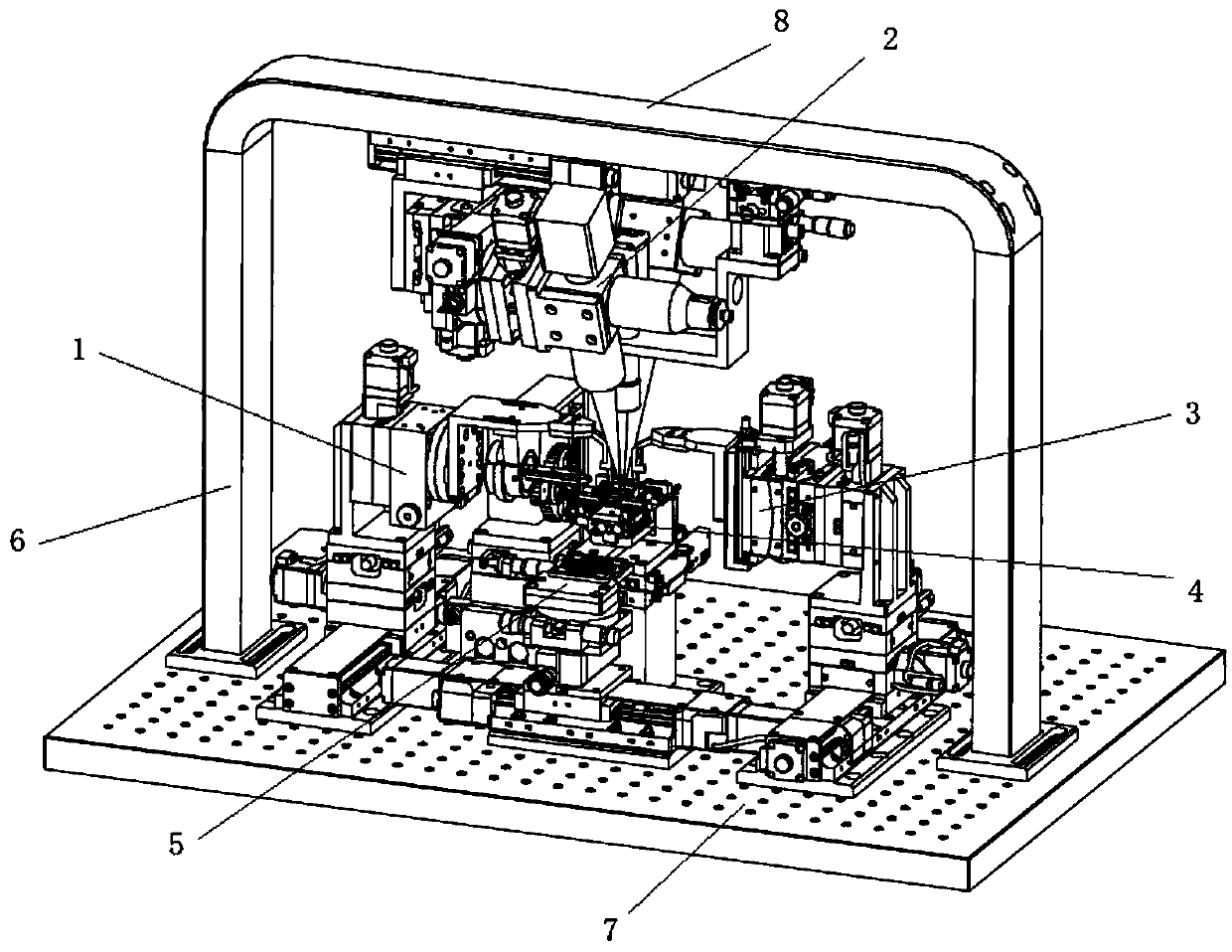
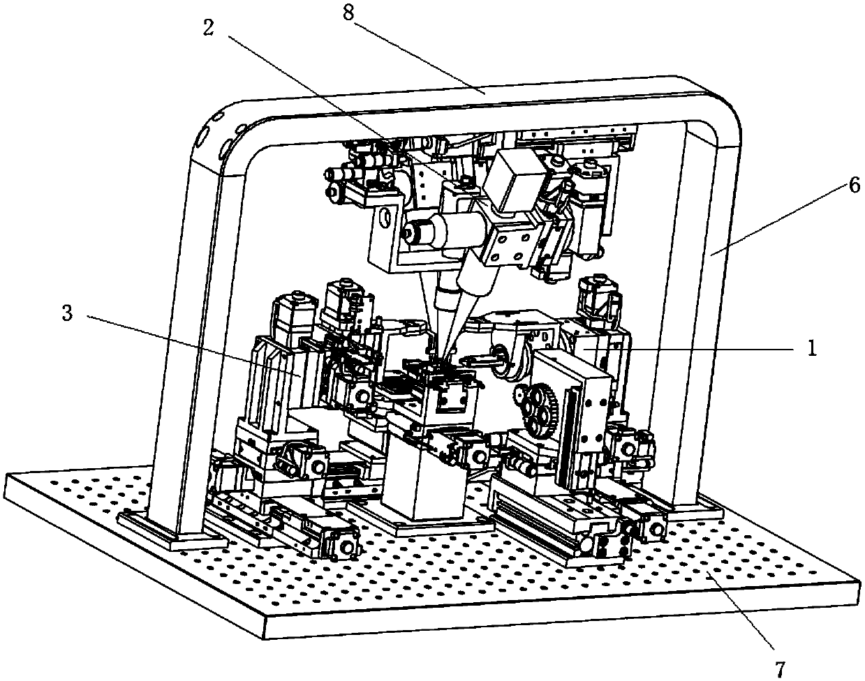
[0074] Such as figure 1 and 2 As shown, this embodiment provides a butterfly semiconductor laser automatic coupling and packaging equipment, including a column 6, a beam 8, and an optical fiber clamp 1, a lens clamp mechanism 3, a lower clamp device 4, and a material tray mechanism arranged on a base 7 5. And a laser power meter 9, an optical fiber automatic angle adjustment welding device 2 is arranged on the beam 8, the optical fiber clamp 1 and the lens clamp mechanism 3 are arranged oppositely, between the optical fiber clamp 1 and the lens clamp mechanism 3 The lower clamp device 4 is set, and the material tray mechanism 5 is set on one side of the l...


PUM


Abstract

The invention discloses a butterfly-shaped semiconductor laser automatic coupling packaging device and relates to the automatic coupling packing field of an electronic device. The automatic coupling packaging device includes a column, a cross beam, and a fiber clamp, a lens clamp mechanism, a lower clamp device and a material disc mechanism arranged on a base, and a laser power meter, wherein thefiber clamp, the lens clamp mechanism and a fiber automatic angle adjusting welding device can be adjusted in position to realize accurate coupling and packaging of a butterfly-shaped semiconductor laser. The device is advantaged in that the structure design is reasonable, the whole subsequent operation from coupling, alignment and packaging can be automatically completed, compared with a traditional hand-operated production line, advantages of high automatic degree, simple and convenient operation, high production efficiency, low production cost and stable product quality are achieved.

Description

technical field [0001] The invention relates to the technical field of automatic coupling and packaging, in particular to automatic coupling and packaging equipment for butterfly semiconductor lasers. Background technique [0002] With the development of optical fiber communication and optical fiber sensing technology, the preparation of optoelectronic devices has become the key to the progress of optical information technology. In optical communication products, the demand for optoelectronic devices such as butterfly semiconductor lasers is increasing with the development. Butterfly semiconductor lasers are the most commonly used long-distance transmission optical signal amplification devices in the optical fiber communication industry, but the packaging cost of butterfly semiconductor lasers has always been high. The huge contradiction has greatly limited the development speed of the optoelectronic device industry. [0003] The biggest bottleneck in the optoelectronic de...

Claims


Application Information

Patent Timeline
IPC IPC(8): G02B6/42
Inventor 段吉安唐佳彭晋文周海波卢胜强徐聪
Owner CENT SOUTH UNIV
Why Eureka
Try Eureka