Radiation-detecting structures
- Summary
- Abstract
- Description
- Claims
- Application Information
AI Technical Summary
Benefits of technology
Problems solved by technology
Method used
Image

Examples
Embodiment Construction
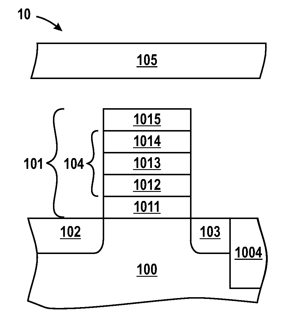
[0021]FIG. 1 includes a cross-sectional illustration of a portion of a radiation detecting device 10 that includes a radiation-detecting structure that can be used in accordance with an embodiment to detect radiation. As illustrated, the radiation detecting device 10 includes a substrate 100, generally suitable for supporting components. The substrate 100 can include a semiconductor material or insulative material, or any combination thereof. For example, the workpiece can include a monocrystalline semiconductor wafer, semiconductor-on-insulator (SOI) wafer, a flat panel display (e.g., a silicon layer over a glass plate), or other substrates conventionally used to form electronic devices. In accordance with a particular embodiment, the substrate 100 is made of a single crystal material, such as a single crystal silicon wafer. Furthermore, the substrate 100 can include a dopant, such as including a n-type or p-type dopant. Substrate 100 can include electronic components or portions o...
PUM
 Abstract
Description
Claims
Application Information
 - R&D Engineer
- R&D Manager
- IP Professional
- Industry Leading Data Capabilities
- Powerful AI technology
- Patent DNA Extraction
Browse by: Latest US Patents, China's latest patents, Technical Efficacy Thesaurus, Application Domain, Technology Topic.
© 2024 PatSnap. All rights reserved.Legal|Privacy policy|Modern Slavery Act Transparency Statement|Sitemap