Field effect transistor with alternate electrical contacts

Inactive Publication Date: 2010-06-24
COMMISSARIAT A LENERGIE ATOMIQUE ET AUX ENERGIES ALTERNATIVES
View PDF13 Cites 22 Cited by
  • Summary
  • Abstract
  • Description
  • Claims
  • Application Information

AI Technical Summary

Benefits of technology

[0018]This invention can improve the integration density of a field effect transistor like a FinFET with disconnected gates, by relaxing the constraint on the dimensions of the electrical contacts, and only connecting one gate out of two per face.

Problems solved by technology

Therefore, it can be seen that rules for the design of electrical contacts are restrictive and limit the integration density of such transistors in this type of structure.

Method used


Image

  • Field effect transistor with alternate electrical contacts
  • Field effect transistor with alternate electrical contacts
  • Field effect transistor with alternate electrical contacts

Examples


Embodiment Construction

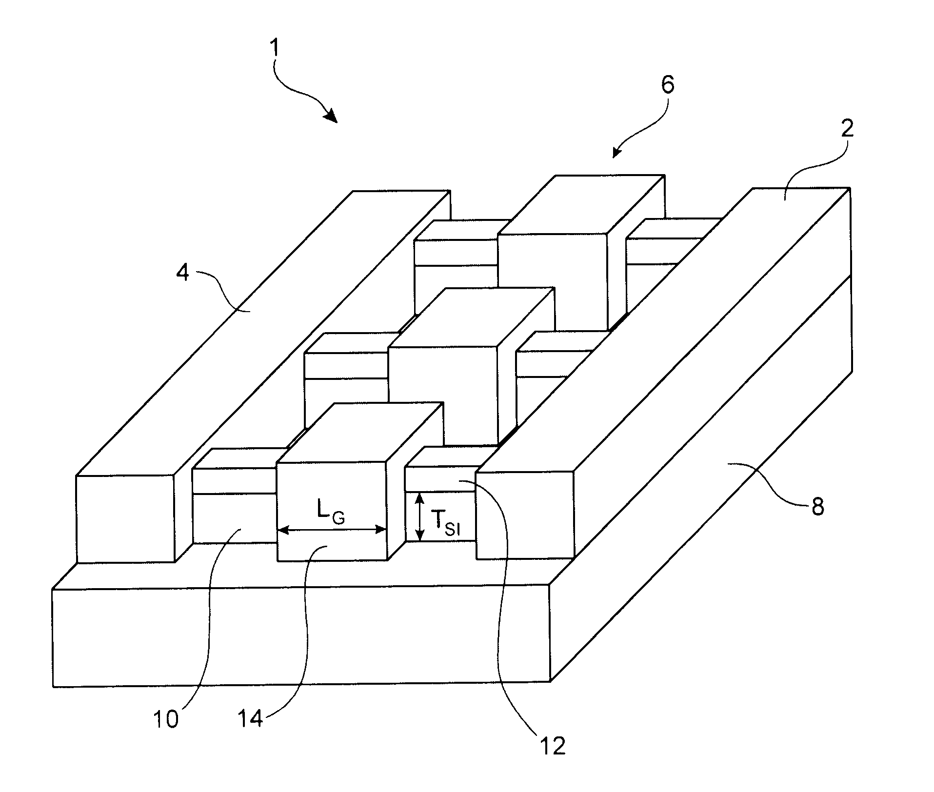
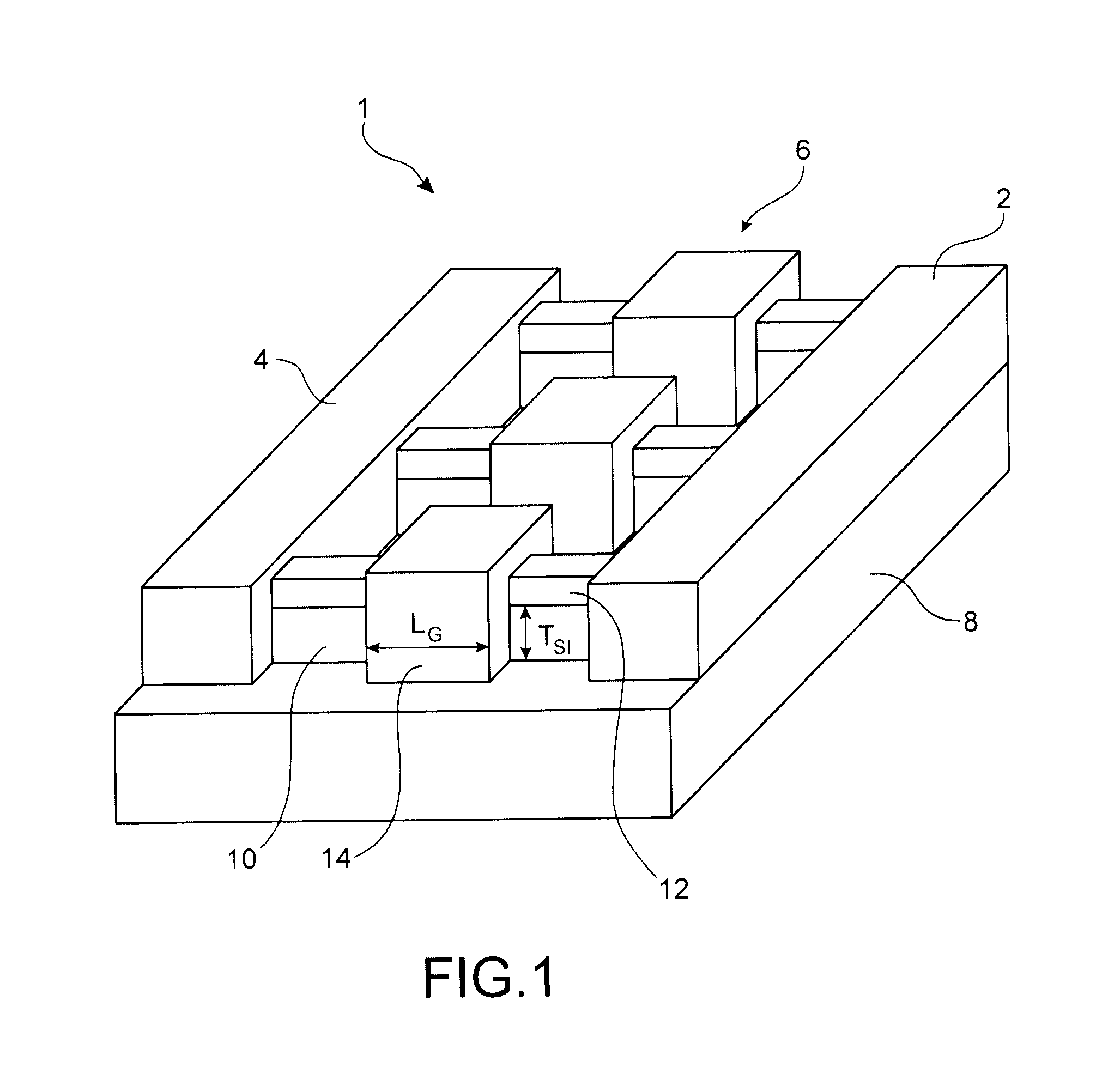
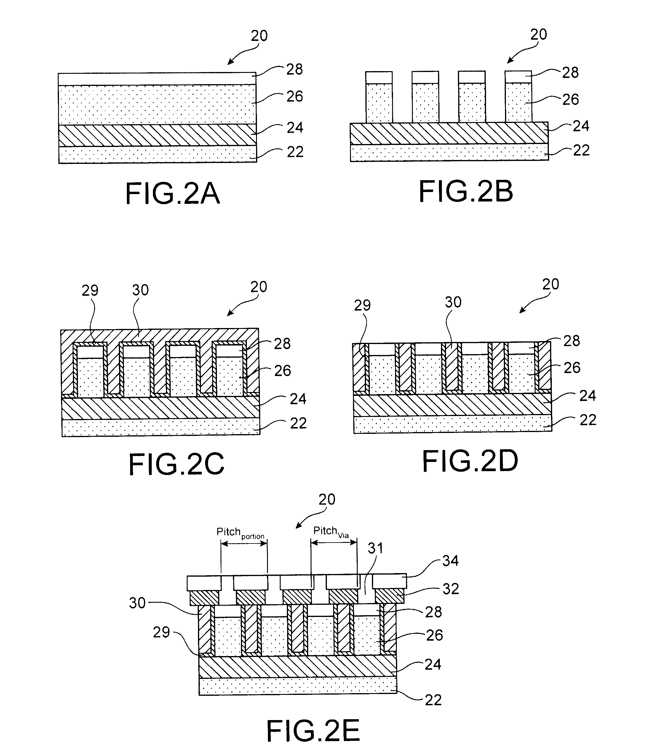
[0013]One purpose of this invention is to disclose a field effect transistor with better integration density.

[0014]To achieve this, this invention discloses a field effect transistor comprising at least:[0015]a support layer,[0016]an active zone based on at least one semiconductor, designed to form a channel, arranged on one face of the support layer, between a first gate and a second gate made on said face of the support layer and each comprising a first face on the side of the support layer and a second face opposite the first face,[0017]a first electrical contact made on the second face of the first gate and electrically connected to the second face of the first gate, and a second electrical contact passing through the support layer and electrically connected to the first face of the second gate.

[0018]This invention can improve the integration density of a field effect transistor like a FinFET with disconnected gates, by relaxing the constraint on the dimensions of the electrical...


PUM


Abstract

A field effect transistor including: a support layer, a plurality of active zones based on a semiconductor, each active zone configured to form a channel and arranged between two gates adjacent to each other and consecutive, the active zones and the gates being arranged on the support layer, each gate including a first face on the side of the support layer and a second face opposite the first face. The second face of a first of the two gates is electrically connected to a first electrical contact made on the second face of the first of the two gates, and the first face of a second of the two gates is electrically connected to a second electrical contact passing through the support layer. The gates of the transistor are not electrically connected to each other.

Description

TECHNICAL FIELD AND PRIOR ART[0001]The invention relates to field effect transistors and particularly FinFET (Fin Field Effect Transistors).[0002]So-called “multi-gate” devices, for example such as FinFETs, have been developed to overcome the disadvantages related to the reduction in the size of CMOS transistors and particularly the increase in energy consumption due to leaks in these transistors and the increase in technological constraints. FinFET transistors provide better electrostatic control than CMOS transistors, giving a better slope under the threshold and therefore a lower leakage current in the blocked state, and a higher current in the conducting state due to the existence of several transport channels. In particular, these gates may be independent of each other, for example so that the threshold voltage can be modulated by means of the second gate.[0003]FIG. 1 shows an example of a FinFET 1. The FinFET 1 comprises a source 2, a drain 4 and n fingers 6 each forming two c...

Claims


Application Information

Patent Timeline
IPC IPC(8): H01L27/12H01L21/762
CPCH01L29/41791H01L29/7855H01L29/66795
Inventor MAYER, FREDERICCLAVELIER, LAURENTPOIROUX, THIERRYBILLIOT, GERARD
Owner COMMISSARIAT A LENERGIE ATOMIQUE ET AUX ENERGIES ALTERNATIVES
Why Eureka
Try Eureka