Liquid crystal display unit and electronic device

Active Publication Date: 2010-06-24
JAPAN DISPLAY WEST
View PDF14 Cites 1 Cited by
  • Summary
  • Abstract
  • Description
  • Claims
  • Application Information

AI Technical Summary

Benefits of technology

[0012]According to the liquid crystal display unit and the electronic device of the embodiments of the invention, the thickness of the under-layered insulation film in the spacer region is smaller than that of the under-layered insulation film in the region other than the spacer region, and thereby the compressive deformation amount of the under-layered insulation film is decreased. Thus, a crack and a fracture in the pixel electrode, the pixel insulation film, the common electrode, and the under-layered insulation film are able to be inhibited from being generated. Therefore, generation of a pixel defect due to pressing the display face is decreased, and reliability is able to be improved.
[0013]Further, in addition to the foregoing structure, in the case where the thickness of the pixel insulation film in the spacer region is larger than the thickness of the pixel insulation film in the region other than the spacer region, the film strength of the pixel insulation film itself is improved. Thus, generation of a pixel defect due to a crack and a fracture is able to be more effectively inhibited.

Problems solved by technology

However, for example, in the case where the spacer is arranged inside the pixel, specific studies have not been made much on appropriate arrangement position of the spacer in the pixel, appropriate structures thereof and the like.
In particular, such a problem becomes significant in the case where the thickness of the pixel insulation film 106 is decreased to heighten the pixel electric field.
In such a liquid crystal display unit having the capture function, in particular, the screen is frequently touched with a finger or the like, and thus there is a high possibility that the foregoing problem that the pixel defect resulting from applying pressure on the screen is generated.

Method used


Image

  • Liquid crystal display unit and electronic device
  • Liquid crystal display unit and electronic device
  • Liquid crystal display unit and electronic device

Examples


first embodiment

1. First Embodiment

Structure of Liquid Crystal Display Unit

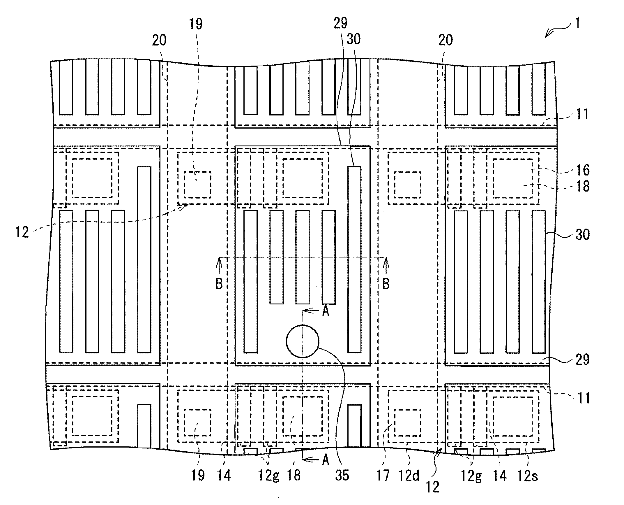
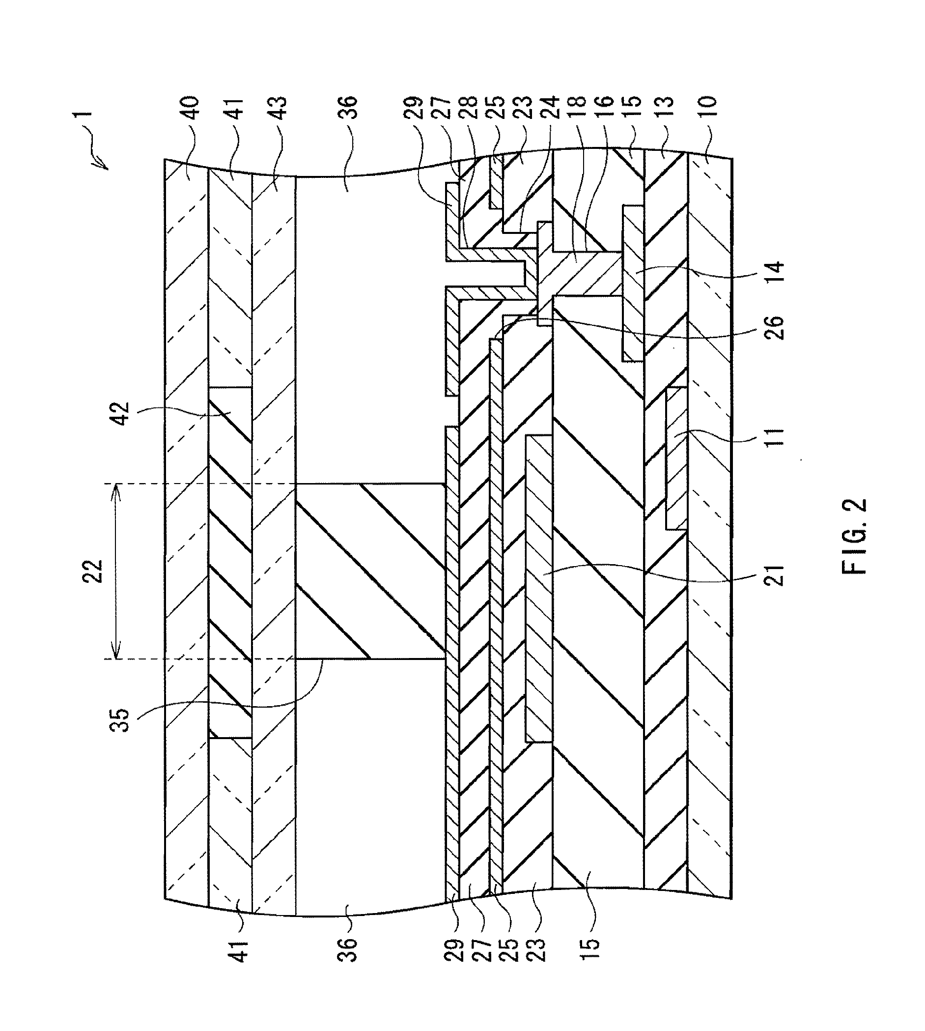
[0032]FIG. 1 illustrates a planar structure of a substantial part of a liquid crystal display unit according to a first embodiment. FIG. 1 illustrates a state after omitting elements located above the liquid crystal layer. FIG. 2 illustrates a cross sectional structure taken along line A-A of FIG. 1.

[0033]As illustrated in FIG. 2, a liquid crystal display unit 1 includes a first glass substrate 10 and a second glass substrate 40. On the first glass substrate 10 side, a thin film transistor (TFT) 12 is provided for every pixel, and a pixel electrode 29 and a common electrode 25 are provided so that a pixel insulation film 27 is sandwiched between the pixel electrode 29 and the common electrode 25.

[0034]A detailed structure of the liquid crystal display unit 1 is as follows.

[0035]On the first glass substrate 10, a plurality of gate lines 11 as a selection line are extendedly provided in a row direction (horizontal direction in...

modified examples

[0067]While the first embodiment has been hereinbefore described, various modifications may be made for the liquid crystal display unit 1 of this embodiment.

[0068]For example, in the foregoing embodiment, the description has been given of the case that in the spacer region 22, the pedestal 21 is arranged in the lowermost layer of the interlayer insulating film 23. However, the pedestal 21 may be arranged at least in part of the interlayer insulating film 23 in the thickness direction. That is, as illustrated in FIG. 6A, the pedestal 21 may be arranged in the uppermost section of the interlayer insulating film 23, or as illustrated in FIG. 6B, the pedestal 21 may be arranged in the intermediate section of the interlayer insulating film 23 in the thickness direction. Further, as illustrated in FIG. 7, the whole interlayer insulating film 23 in the thickness direction in the spacer region 22 may be substituted with the pedestal 21.

[0069]Further, in the foregoing embodiment, the descrip...

second embodiment

Structure and Action of Liquid Crystal Display Unit

[0071]FIG. 9 illustrates a cross sectional structure of a liquid crystal display unit according to a second embodiment. A liquid crystal display unit 2 is different from the liquid crystal display unit 1 of the first embodiment mainly in the structure of a pixel insulation film 50. The thickness in the spacer region 22 in the pixel insulation film 50 is formed larger than the thickness in the other regions. That is, the pixel insulation film 50 is in the upward and downward convex shape. The thickness of the interlayer insulating film 23 in the spacer region 22 is smaller than that of the interlayer insulating film 23 in the other regions, and strength to pressure is increased therein. Thus, the deformation amount of the common electrode 25, the pixel insulation film 50, and the pixel electrode 29 in the spacer region 22 becomes small. In particular, since the pixel insulation film 50 in the spacer region 22 is in the downward conve...


PUM


Abstract

A liquid crystal display unit includes: a first substrate having an under-layered insulation film, a common electrode formed on the under-layered insulation film, and a pixel electrode formed over the common electrode with a pixel insulation film in between; a second substrate provided on pixel electrode side of the first substrate so as to oppose thereto; a liquid crystal layer provided between the first substrate and the second substrate; and a spacer provided to retain a distance between the first substrate and the second substrate, in such a manner that one end of the spacer is contacted with a top face of the pixel electrode. A thickness of the under-layered insulation film in a spacer region which is defined as a region occupied by the spacer is smaller than a thickness of the under-layered insulation film in a region other than the spacer region.

Description

BACKGROUND OF THE INVENTION[0001]1. Field of the Invention[0002]The present invention relates to a liquid crystal display unit performing display by transverse electric field mode liquid crystal and an electronic device including the same.[0003]2. Description of the Related Art[0004]As one type of liquid crystal display units, there is a liquid crystal display unit in which transverse electric field mode liquid crystal such as FFS (fringe field switching) mode is used. FIG. 15 illustrates a cross sectional section of enlarged part of an FFS mode liquid crystal display unit 100. The FFS mode liquid crystal display unit 100 includes two glass substrates 101a and 101b composing a liquid crystal display panel. A spacer 102 determining a distance between the glass substrates 101a and 101b is arranged between one glass substrate 101a and the other glass substrate 101b. On the one glass substrate 101a side, a thin film transistor 103 is formed. On the thin film transistor 103, an interlaye...

Claims


Application Information

Patent Timeline
IPC IPC(8): G02F1/1333
CPCG02F1/13394G02F1/133345
Inventor YAGI, KEIICHIKANAYA, YASUHIRO
Owner JAPAN DISPLAY WEST
Why Eureka
Try Eureka