Inspecting apparatus, and inspecting method
- Summary
- Abstract
- Description
- Claims
- Application Information
AI Technical Summary
Benefits of technology
Problems solved by technology
Method used
Image

Examples
first embodiment
[0039]Hereinafter, a first embodiment of the invention will be described in detail with reference to the drawings.
Configuration of Inspecting Apparatus
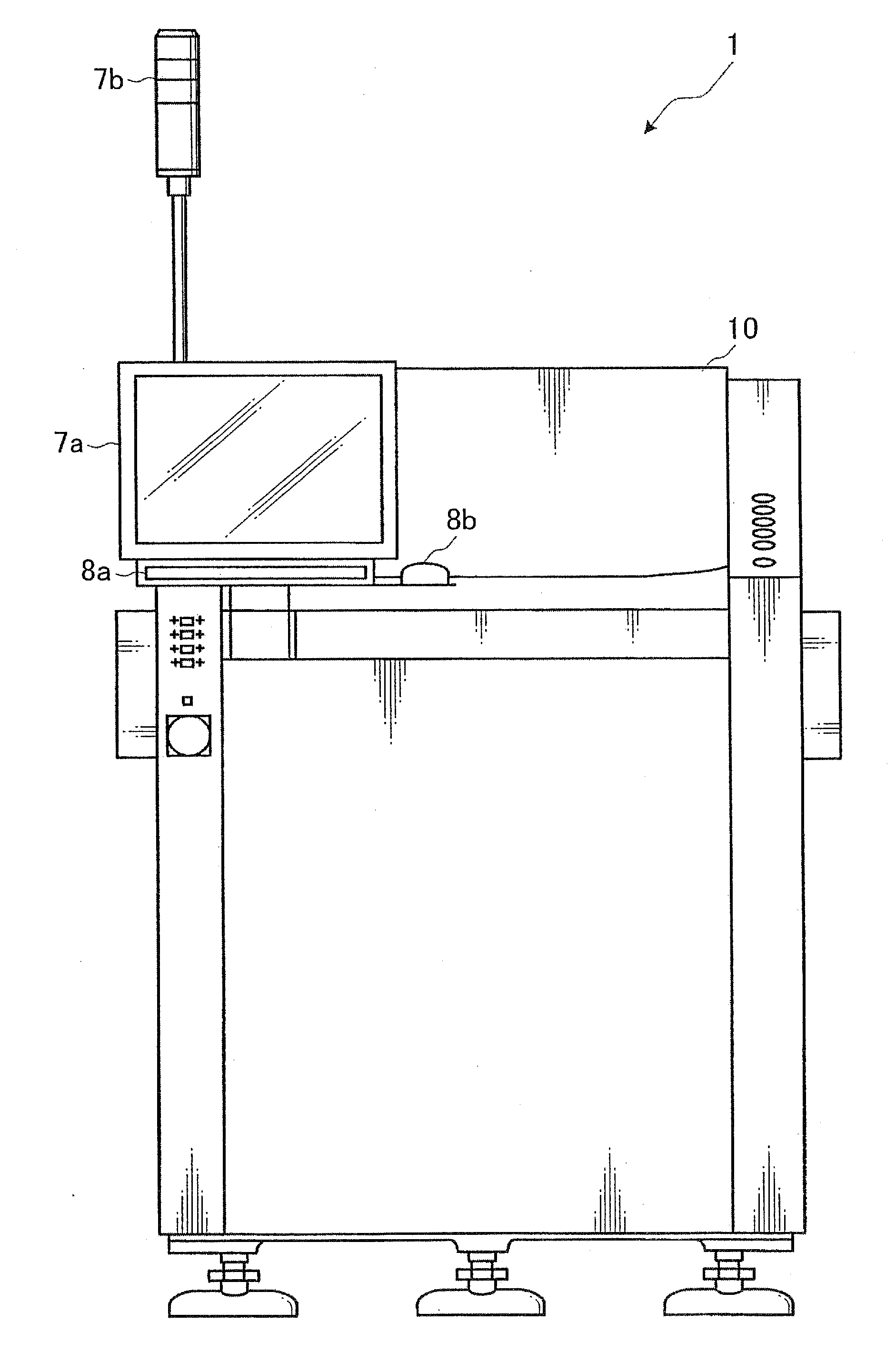
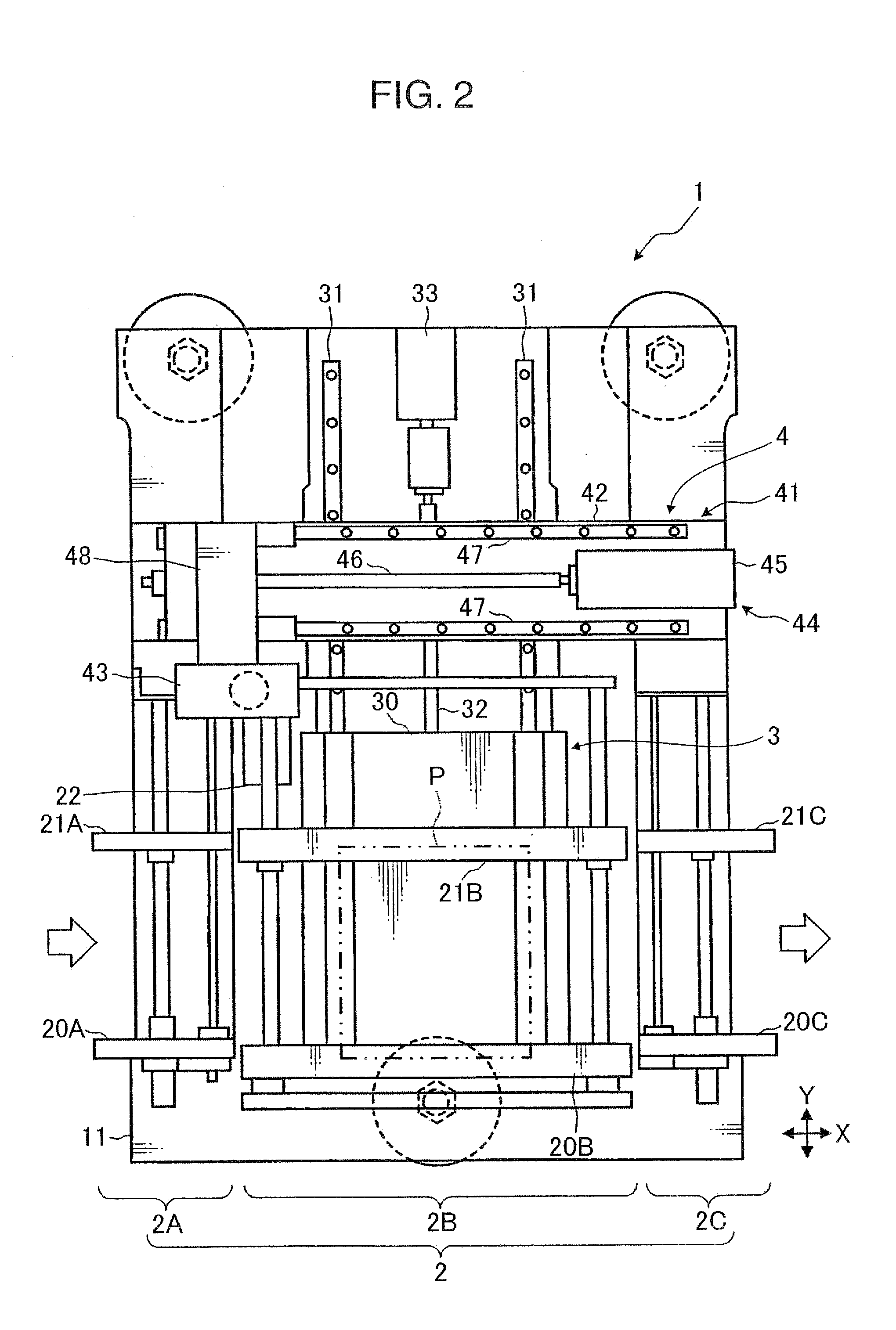
[0040]As are shown in FIG. 1 and FIG. 2, an inspecting apparatus 1 of this embodiment is covered by a cover 10 almost in the shape of a square prism as a whole and has a hollow base stand 11 almost in the shape of a square prism inside the cover 10. As shown in FIG. 1 through FIG. 3, the inspecting apparatus 1 configured as above includes a board transportation portion 2, a table transportation 3, an image taking device transportation portion 4, an illumination device 5 (illuminator), an image taking device 6, a display device 7, an input device 8, and a control device 9.
[0041]As shown in FIG. 2, the board transportation portion 2 is provided on the base stand 11 to transport a printed wiring board P (hereinafter, referred to as the board P) as a subject to be inspected, and it is comprised by three parts each having a pair of belt co...
first modification
[0100]A first modification of the first embodiment will now be described. In this modification, a filter 61 is provided to the image taking device 6 of the first embodiment above. Accordingly, like components as those in the first embodiment above are referred to under the same names and labeled with like reference numerals and descriptions thereof are omitted herein where appropriate.
[0101]As shown in FIG. 16, the image taking device 6 is provided with the filter 61 in front of the taking plane. The filter 61 is comprised by a filter that does not transmit infrared light having light intensity identical to the light intensity of the surface reflected light. Accordingly, when the image taking device 6 takes an image of reflected light, which is infrared light irradiated from the illumination device 5 and reflected on the board, the surface reflected light is eliminated by the filter 61. It thus becomes possible to obtain a captured image excluding the surface reflected light.
[0102]A...
second modification
[0104]A second modification of the first embodiment above will now be described. In this modification, the attachment angles of the illumination device 5 and the image taking device 6 of the first embodiment above are changed. Accordingly, like components as those in the first embodiment above are referred to under the same names and labeled with like reference numerals and descriptions thereof are omitted herein where appropriate.
[0105]As shown in FIG. 17, the illumination device 5 and the image taking device 6 are disposed above the board P on the surface side and disposed on the opposite sides with an taking region on the board P to be imaged by the image taking device 6 in between, in other words, on the opposite sides with an axis perpendicular to the surface of the board P in between, in such a manner that each is diagonal with respect to the board P. Specifically, the illumination device 5 and the image taking device 6 are in a mirror relation with respect to the perpendicula...
PUM
 Abstract
Description
Claims
Application Information
 - R&D
- Intellectual Property
- Life Sciences
- Materials
- Tech Scout
- Unparalleled Data Quality
- Higher Quality Content
- 60% Fewer Hallucinations
Browse by: Latest US Patents, China's latest patents, Technical Efficacy Thesaurus, Application Domain, Technology Topic, Popular Technical Reports.
© 2025 PatSnap. All rights reserved.Legal|Privacy policy|Modern Slavery Act Transparency Statement|Sitemap|About US| Contact US: help@patsnap.com