Substrate treatment apparatus, substrate treatment method and storage medium

Inactive Publication Date: 2010-07-01
TOKYO ELECTRON LTD
View PDF6 Cites 7 Cited by
  • Summary
  • Abstract
  • Description
  • Claims
  • Application Information

AI Technical Summary

Benefits of technology

[0016]In accordance with the aspects of the present invention, in the alignment module, the semiconductor wafer can be arranged in the direction set by the recipe setting unit. Accordingly, the portion of the rear surface of the semiconductor wafer supported by the supporting member can be changed whenever the heat treatment is performed in the he

Problems solved by technology

However, when the annealing process is performed twice, since the direction of the wafer transferred to the heat treatment module is not changed and the same portions of the rear surface of the wafer are supported by the supporting pins in the first and seco

Method used


Image

  • Substrate treatment apparatus, substrate treatment method and storage medium
  • Substrate treatment apparatus, substrate treatment method and storage medium
  • Substrate treatment apparatus, substrate treatment method and storage medium

Examples


Example

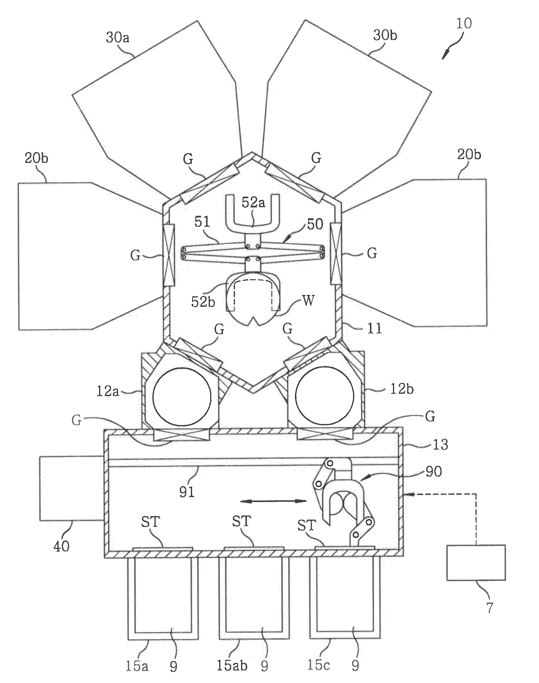
[0029]Hereinafter, an embodiment of the present invention will be described. FIG. 1 is a transversal cross sectional view showing an example of a semiconductor manufacturing apparatus that is a substrate treatment apparatus in accordance with the embodiment of the present invention. In FIG. 1, reference numeral 10 designates a single-wafer semiconductor manufacturing apparatus in which semiconductor wafers (hereinafter, referred to as “wafers”) W are transferred one by one and a predetermined process is performed on each wafer. The semiconductor manufacturing apparatus 10 includes, e.g., two plasma processing modules 20a and 20b and two heat treatment modules 30a and 30b. The plasma processing modules 20a and 20b and the heat treatment modules 30a and 30b are airtightly connected to four sides of a vacuum transfer chamber 11 having a hexagonal transversal cross section, respectively. Further, one of the plasma processing modules 20a and 20b and one of the heat treatment modules 30a ...


PUM


Abstract

A substrate treatment apparatus eliminates breakage of a wafer W due to having the wafer supported by a supporting member when heat treatment is performed on the wafer W a plurality of times by a heat treatment module. The substrate processing apparatus includes a recipe setting unit for setting process conditions for a process recipe for the semiconductor wafer W and a direction of the semiconductor wafer W, by associating the conditions and the direction with each other. Through the recipe setting unit, the direction of the semiconductor wafer W can be set, and the semiconductor wafer W can be arranged in a direction set by an alignment module. Thus, portions R to be supported by the supporting members 60a, 60b and 60c on the rear surface of the semiconductor wafer can be changed every time the heat treatment module performs heat treatment.

Description

[0001]This application is a Continuation Application of PCT International Application No. PCT / JP2008 / 061639 filed on Jun. 26, 2008, which designated the United States.FIELD OF THE INVENTION[0002]The present invention relates to a technique for performing heat treatment on a semiconductor wafer (hereinafter, referred to as a “wafer”) after a direction of the wafer is aligned in an alignment module.BACKGROUND OF THE INVENTION[0003]In a semiconductor manufacturing process, a semiconductor manufacturing apparatus, called a multi-chamber system, including a plurality of processing modules for performing vacuum processes on wafers one by one is used. The semiconductor manufacturing apparatus generally includes a loading unit of a wafer carrier, an atmospheric transfer chamber connected to the loading unit, a vacuum transfer chamber connected to the atmospheric transfer chamber through a load-lock chamber, and a plurality of processing modules connected to the vacuum transfer chamber. The ...

Claims


Application Information

Patent Timeline
IPC IPC(8): H01L21/683G06F17/50G06F17/00
CPCH01J37/32431H01J2237/2001H01L21/67276H01L21/67745H01L21/683H01L21/3065H01L21/68H01L21/205
Inventor SEKIDO, KOICHIMAEKAWA, KOJITAKANO, KUNIO
Owner TOKYO ELECTRON LTD
Why Eureka
Try Eureka