

Photoelectric converter
- Summary
- Abstract
- Description
- Claims
- Application Information
AI Technical Summary
Benefits of technology
Problems solved by technology
Method used
Image

Examples
Embodiment Construction
[0060]In the following, the best mode for carrying out the present invention is described with reference to accompanying drawings.
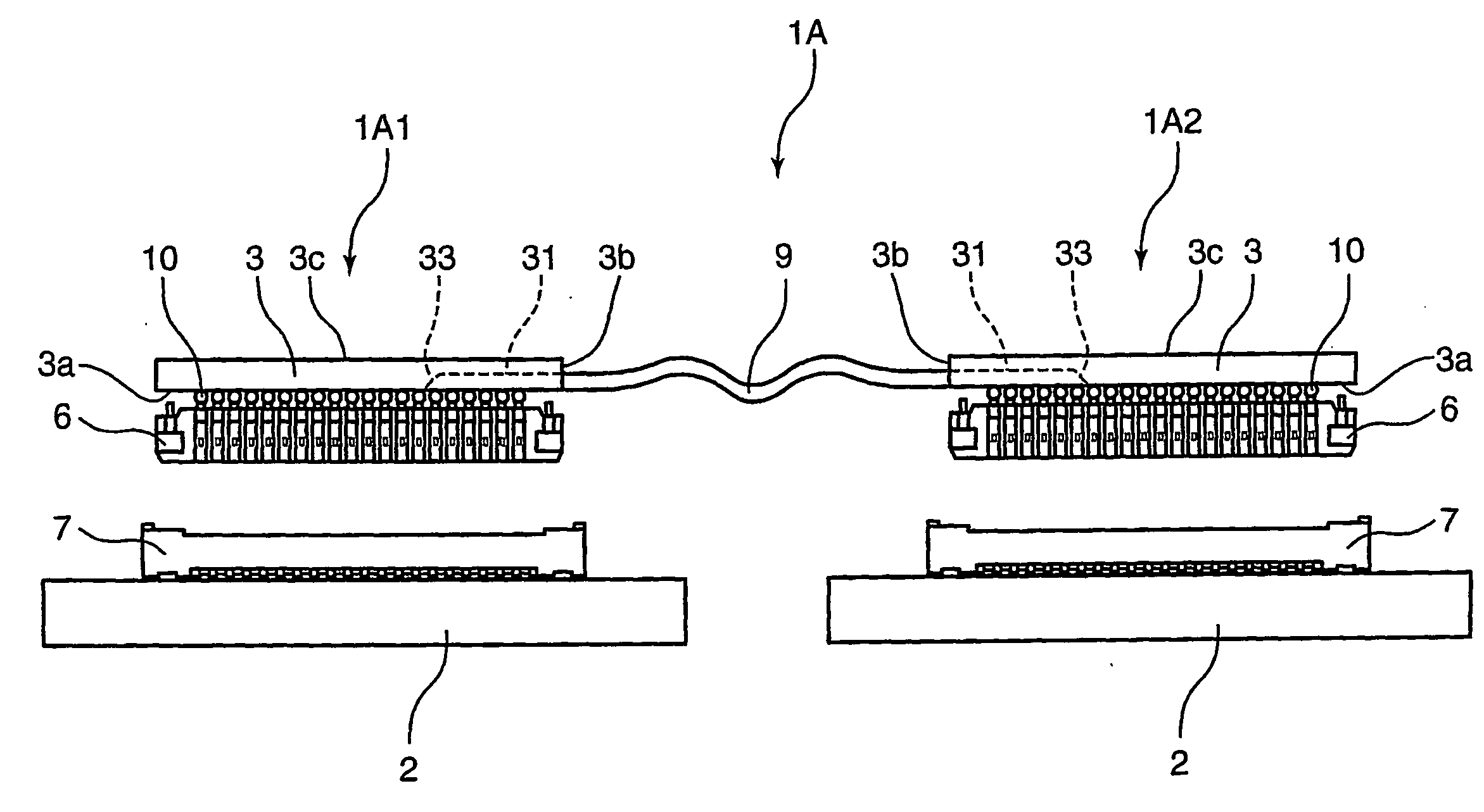
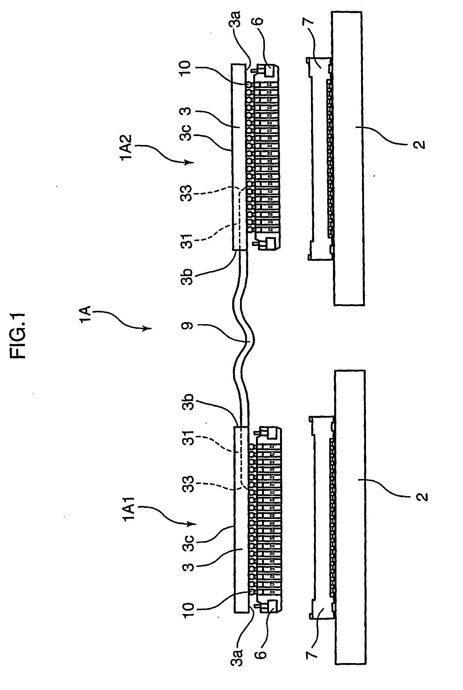
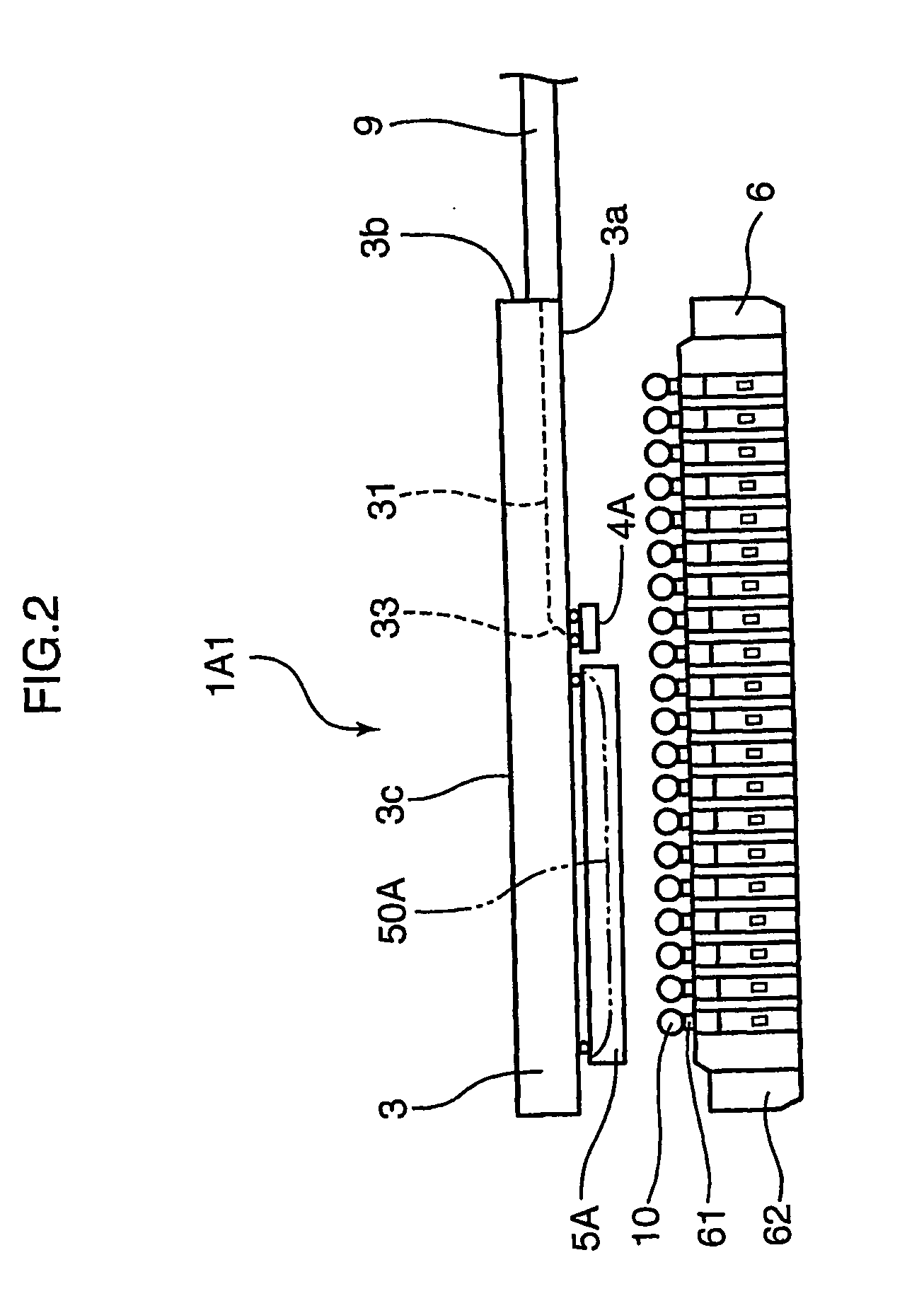
[0061]FIG. 1 shows a photoelectric converter 1A according to a first embodiment of the present invention. The photoelectric converter 1A includes a light emitting side photoelectric converting portion (also referred to as E / O module) 1A1 adapted to be mounted on a wiring substrate 2 by engagement of a header (electric connector) 6 and a socket (electric connector) 7, a light receiving side photoelectric converting portion (also referred to as O / E module) 1A2 adapted to be mounted by engagement of the electric connectors 6 and 7 similarly to the other wiring substrate 2, and an external waveguide 9 adapted to effect an optical coupling between the converting portions 1A1 and 1A2. That is, in the photoelectric converter 1A, the electric converting portion on the other side seen from the light emitting side photoelectric converting portion 1A1 or the light r...
PUM
 Abstract
Description
Claims
Application Information