Electronic devices with improved ohmic contact

Active Publication Date: 2010-02-18
S O I TEC SILICON ON INSULATOR THECHNOLOGIES
View PDF10 Cites 12 Cited by
  • Summary
  • Abstract
  • Description
  • Claims
  • Application Information

AI Technical Summary

Benefits of technology

[0027]Formation of the alloy does in fact enable the band diagram under the contact t

Problems solved by technology

But etching is tricky to perform as it may generate defects on the etching sides which will minimize the performances of the component (surface leakage current, reduction of breakdown voltage).
However, to activate silicon by reorganization of the crystalline structure after implantation, very high temperature annealing is required (1500° C. under 100 bars of N2), and this type of method is difficult to apply on an industrial scale.
But this method comprises two drawbacks which are at the origin of leakage currents reducing the efficiency of the device: firstly the superficial layer has to be eliminated, and secondly the

Method used


Image

  • Electronic devices with improved ohmic contact
  • Electronic devices with improved ohmic contact
  • Electronic devices with improved ohmic contact

Examples


example 1

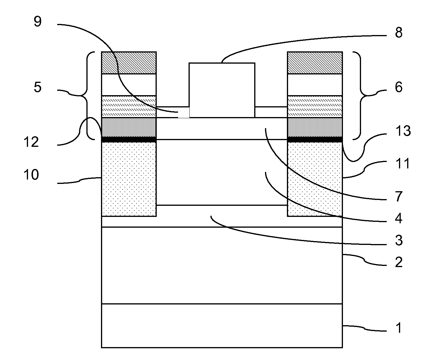
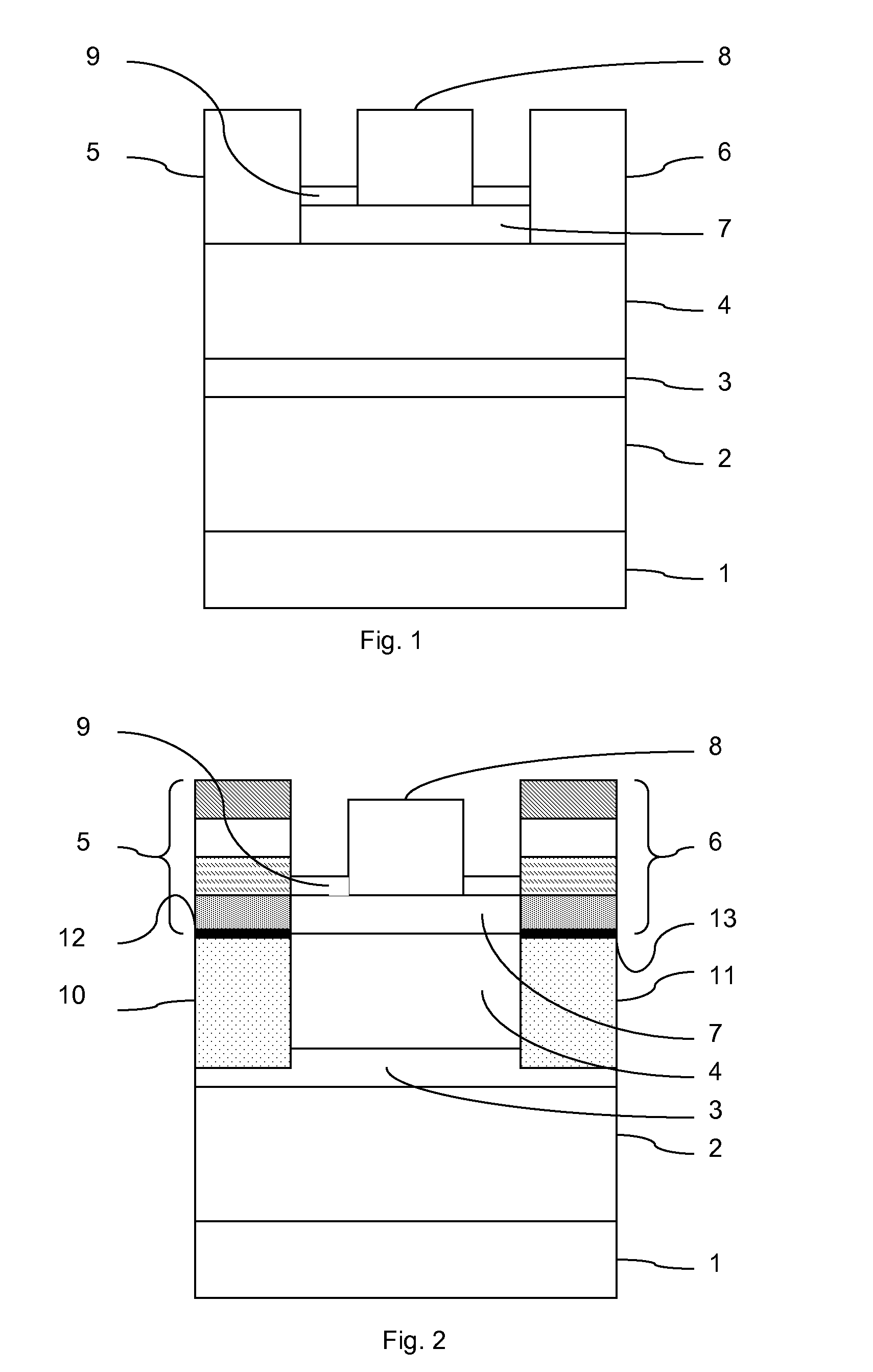
[0087]A structure successively comprising a semi-conductor layer 1, a buffer layer 2, a channel layer 3 to contain an electron gas, a barrier layer 4 and a superficial layer 7 is first of all formed by a known technique such as MBE or MOCVD.

[0088]The barrier layer is made of AlGaN and presents an aluminium content comprised between 10 and 25%.

[0089]Implantation of aluminium at high dose is then performed in barrier layer 4 so as to achieve an aluminium content of more than 1019 atoms per cm3 at the level of the surface of barrier layer 4 in the lattice of the material. The implanted metal content can be up to 1021 atoms per cm3.

[0090]Annealing according to the second alternative embodiment described above is then performed. For this purpose, the structure thus obtained is subjected to a temperature of 700° C. for 30 minutes in a NH3:N2 atmosphere (respectively in proportions ⅓:⅔).

[0091]Etching of the superficial layer is then performed at the location scheduled for the drain and sou...

example 2

[0093]A structure successively comprising a semi-conductor layer 1, a buffer layer 2, a channel layer 3 to contain an electron gas, a barrier layer 4 and a superficial layer 7 is first of all formed by a known technique such as MBE or MOCVD.

[0094]The barrier layer is made of AlGaN and presents an aluminium content comprised between 10 and 25%.

[0095]Etching of the thickness of superficial layer 7 and of one third of barrier layer 4 is then performed at the location of source 5 and drain 6. For this, techniques known to the person skilled in the trade are used, such as formation of a mask followed by performing dry etching or wet method etching, for example KOH-based activated by UV.

[0096]Aluminium is then implanted at reduced dose so as to obtain an implantation profile with a maximum at the surface of barrier layer 4. The implanted aluminium content varies from 1019 to 1021 atoms per cm3.

[0097]Formation of the electrodes is then performed in the same way as in example 1.

[0098]The re...

example 3

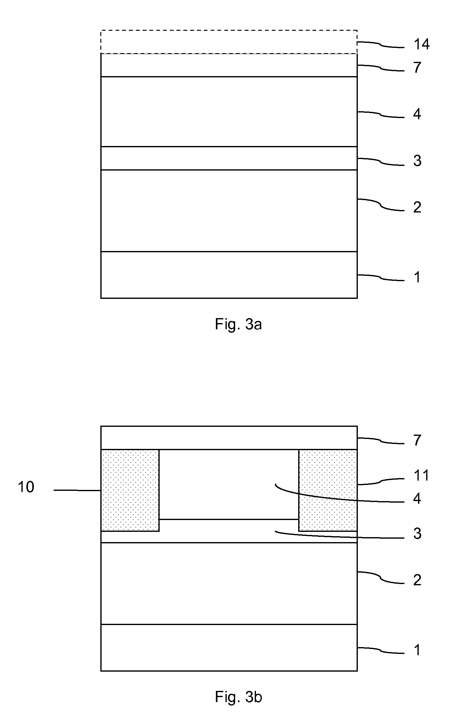
[0100]A structure successively comprising a semi-conductor layer 1, a buffer layer 2, a channel layer 3 to contain an electron gas, a barrier layer 4 and a superficial layer 7 is first of all formed by a known technique such as MBE or MOCVD.

[0101]The barrier layer is made of AlGaN and presents an aluminium content comprised between 10 and 25%.

[0102]An encapsulating protective layer 14 made from a material such as SiO2 or Si3N4 for example is then formed on this structure.

[0103]Co-implantation of aluminium and silicon is then performed so as to reach an aluminium content of more than 1019 atoms per cm3 at the level of the surface of barrier layer 4 in the material lattice. The implanted aluminium+silicon content can be up to 1021 atoms per cm3.

[0104]Annealing of this structure is then performed at a temperature of 1050° C. for 30 minutes in a N2 atmosphere, the surface being protected by the encapsulating layer used for implantation.

[0105]Encapsulating protective layer 14 is then rem...


PUM


Abstract

In one embodiment, the disclosure relates to an electronic device successively comprising from its base to its surface: (a) a support layer, (b) a channel layer adapted to contain an electron gas, (c) a barrier layer and (d) at least one ohmic contact electrode formed by a superposition of metallic layers, a first layer of which is in contact with the barrier layer. The device is remarkable in that the barrier layer includes a contact region under the ohmic contact electrode(s). The contact region includes at least one metal selected from the metals forming the superposition of metallic layers. Furthermore, a local alloying binds the contact region and the first layer of the electrode(s).

Description

CROSS-REFERENCE TO RELATED APPLICATIONS[0001]This patent application is a continuation of and claims priority to International Application No. PCT / IB2008 / 000788, filed Mar. 25, 2008, which in turn claims priority to French Patent Application No. 0754186, filed on Mar. 30, 2007. Each of the aforementioned patent applications in incorporated by reference herein in its entirety.BACKGROUND[0002]1. Field of the Invention[0003]The present invention relates to an electronic device comprising at least one support layer, a channel layer to contain an electron gas, a barrier layer and an ohmic contact electrode formed by a superposition of metallic layers the first of which is in contact with the barrier layer.[0004]2. Description of Related Art[0005]Electronic devices comprising at least one channel layer where an electron gas is able to flow, a barrier layer, and at least one ohmic contact electrode, find numerous applications.[0006]Among these devices, field effect transistors of the High ...

Claims


Application Information

Patent Timeline
IPC IPC(8): H01L29/778H01L21/20H01L21/768
CPCH01L21/28575H01L29/41725H01L29/778H01L29/66462H01L29/452H01L29/45H01L29/417
Inventor LAHRECHE, HACENE
Owner S O I TEC SILICON ON INSULATOR THECHNOLOGIES
Why Eureka
Try Eureka