Method for detecting flash program failures

Active Publication Date: 2010-07-15
MICRON TECH INC
View PDF10 Cites 25 Cited by
  • Summary
  • Abstract
  • Description
  • Claims
  • Application Information

AI Technical Summary

Problems solved by technology

For instance, NAND flash memory devices may sometimes include bad blocks due, for example, to defects that may have occurred during the manufacturing process, and may require error correction to maintain data integrity.
Additionally, flash memory devices may be susceptible to programming failures that may occur during operation.
As will be understood, the failure to successfully program a memory d

Method used


Image

  • Method for detecting flash program failures
  • Method for detecting flash program failures
  • Method for detecting flash program failures

Examples


Embodiment Construction

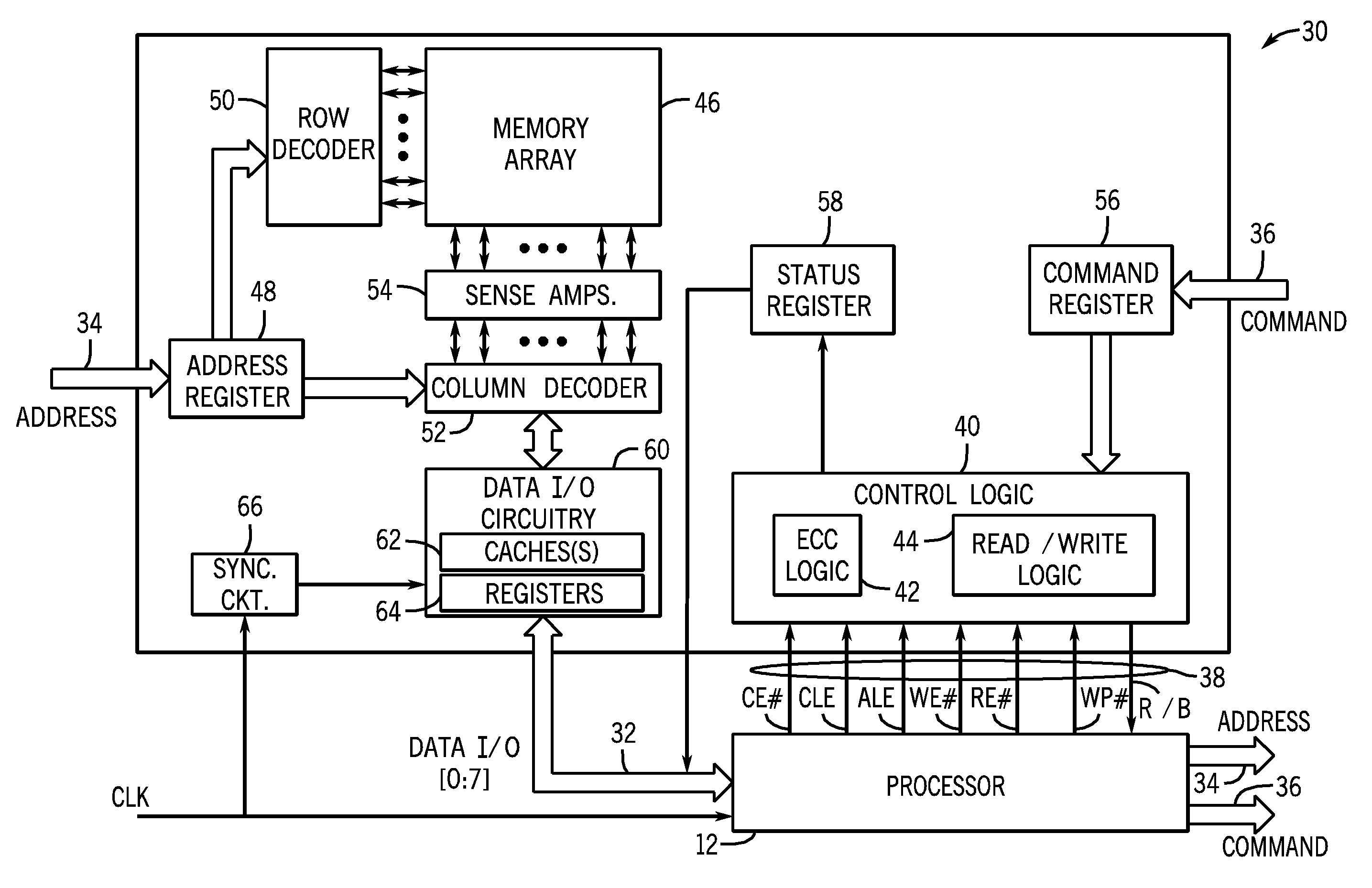
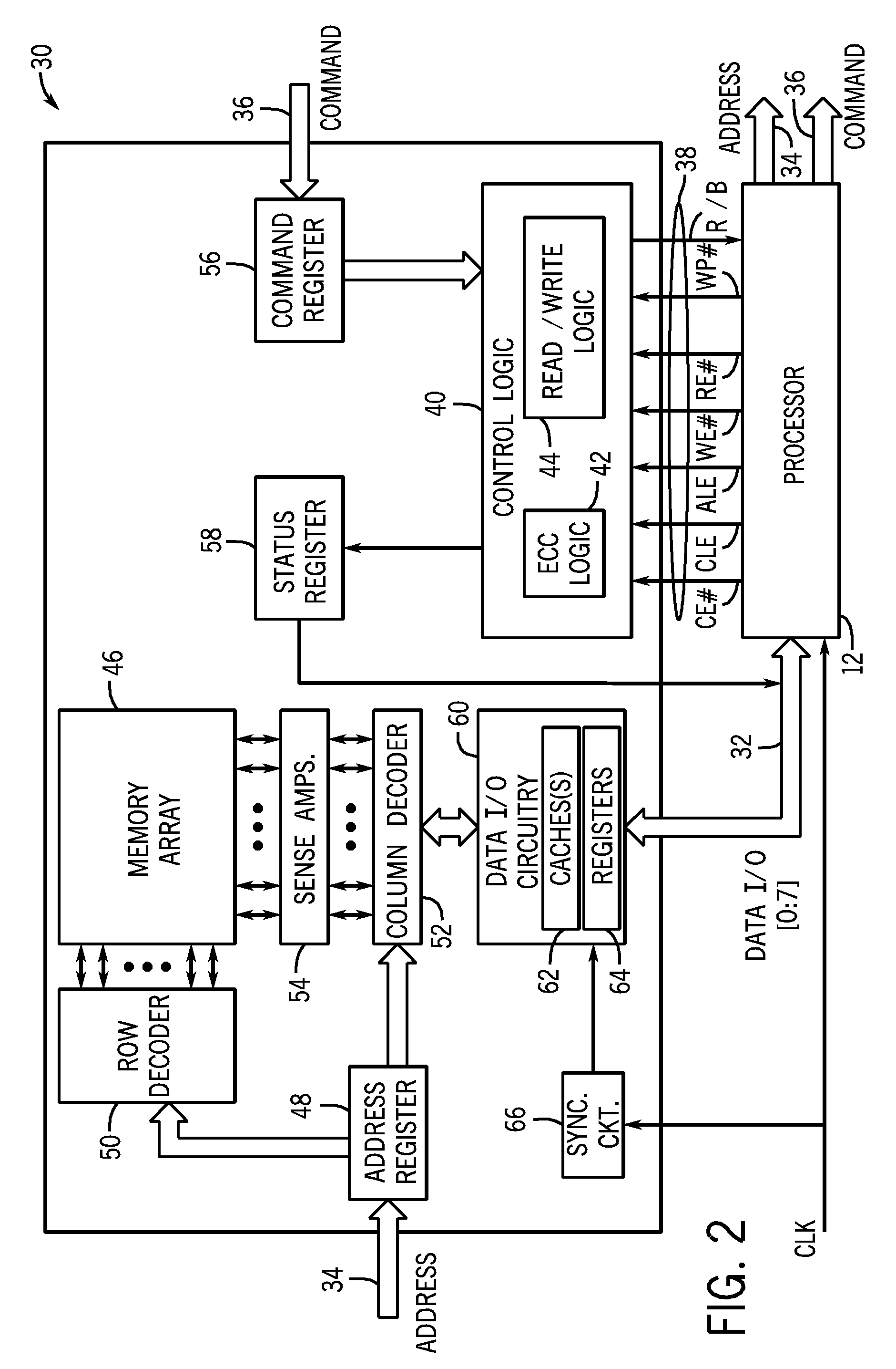
[0016]As discussed in further detail below, one or more embodiments of the present invention provide one or more techniques for the detection of NAND flash programming failures using a single programming operation. One such technique exploits a fundamental principle relating to how flash memory is programmed. Generally, a NAND flash programming operation begins with a fully erased page. Typically, this is accomplished by initiating an erase operation which results in a charge being “erased” from each of the memory cells of the page. In the context of NAND flash memory, an erase operation may include writing the same data value to each of the memory cells in a page. The data value may be a binary logic value, such as a 0 or 1. By way of example, in one embodiment, an erase operation may be viewed as storing a value of “1” for a single level cell (SLC) memory, or a value of “11” for a multiple level cell (MLC), in each of the cells in a page. The programming algorithm then writes a de...


PUM


Abstract

One or more techniques are provided for programming a flash memory device. In one embodiment, the memory device is programmed such that a data pattern written to a page in the memory device has encoded therein an expected count value corresponding to the number of times a first binary value occurs in the data pattern. The data pattern includes the program data and the expected count value, and is written to the page in a single operation. The expected count value may be stored in a count field in the management area of the page. During a page read operation, the expected count value is compared to the actual count of the number of bits having the first binary value in the data area of the page. If the expected count is equal to the actual count, then the program data is determined to be valid.

Description

BACKGROUND[0001]1. Field of the Invention[0002]Embodiments of the invention relate generally to the field of memory devices and, more particularly, to techniques for detecting programming failures in flash memory devices.[0003]2. Description of the Related Art[0004]In recent years, NAND flash memory has become an increasingly popular form of non-volatile storage utilized by various embedded systems and electronic devices, such as portable digital media players, memory cards, USB flash drives, and cellular telephones, to name a few. The increased demand may be attributed, at least partially, to the higher memory densities that NAND flash memory devices typically offer relative to other types of non-volatile memories, such as NOR flash memory. Additionally, NAND flash memory may generally be produced at a lower cost relative to NOR flash memory due, for instance, to the lower number of metal contacts utilized in constructing a NAND flash memory array. Thus, as the demand for lower-pow...

Claims


Application Information

Patent Timeline
IPC IPC(8): G11C16/04G11C16/06G11C7/00
CPCG06F11/1068G11C16/04G11C29/10Y10T29/49002G11C29/42G11C2029/0411G11C29/38
Inventor FEELEY, PETER S.WONG, WANMOPEKNY, THEODORE T.SHAPERO, SAMUEL A.KEAYS, BRADY
Owner MICRON TECH INC
Why Eureka
Try Eureka