Planar waveguide laser device

a laser device and waveguide technology, applied in laser details, optical resonator shape and construction, active medium materials, etc., can solve the problems of laser light oscillation, high gain, and easy oscillation of multiple waveguide modes

Active Publication Date: 2010-07-29
MITSUBISHI ELECTRIC CORP
View PDF4 Cites 10 Cited by
  • Summary
  • Abstract
  • Description
  • Claims
  • Application Information

AI Technical Summary

Benefits of technology

[0009]According to the present invention, a material having a refraction index in a range between the TE polarization refraction index and the TM polarization refraction index of the laser medium is adopted for the clad, and thus either one of TE polarization and TM polarization does not satisfy the total reflection condition. Hence, the laser oscillation can be performed for either one of the polarizations that satisfies the total reflection condition.

Problems solved by technology

However, the gain is high and oscillations easily occur in multiple waveguide modes.
Thus, challenges are to oscillate laser light with linear polarization that is required at the time of wavelength conversion and to oscillate laser light restricted to a desired mode.
Further challenges are to output laser light with high efficiency by reducing amplification of unnecessary light (parasitic amplification) and parasitic oscillation, which occurs by the trapping of light in the waveguide because of the total reflection on the external surfaces and end surfaces of the clad.

Method used


Image

  • Planar waveguide laser device
  • Planar waveguide laser device
  • Planar waveguide laser device

Examples


first embodiment

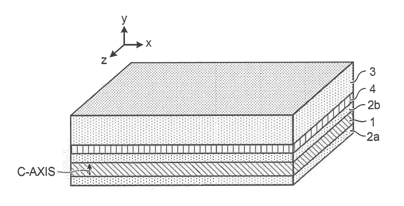
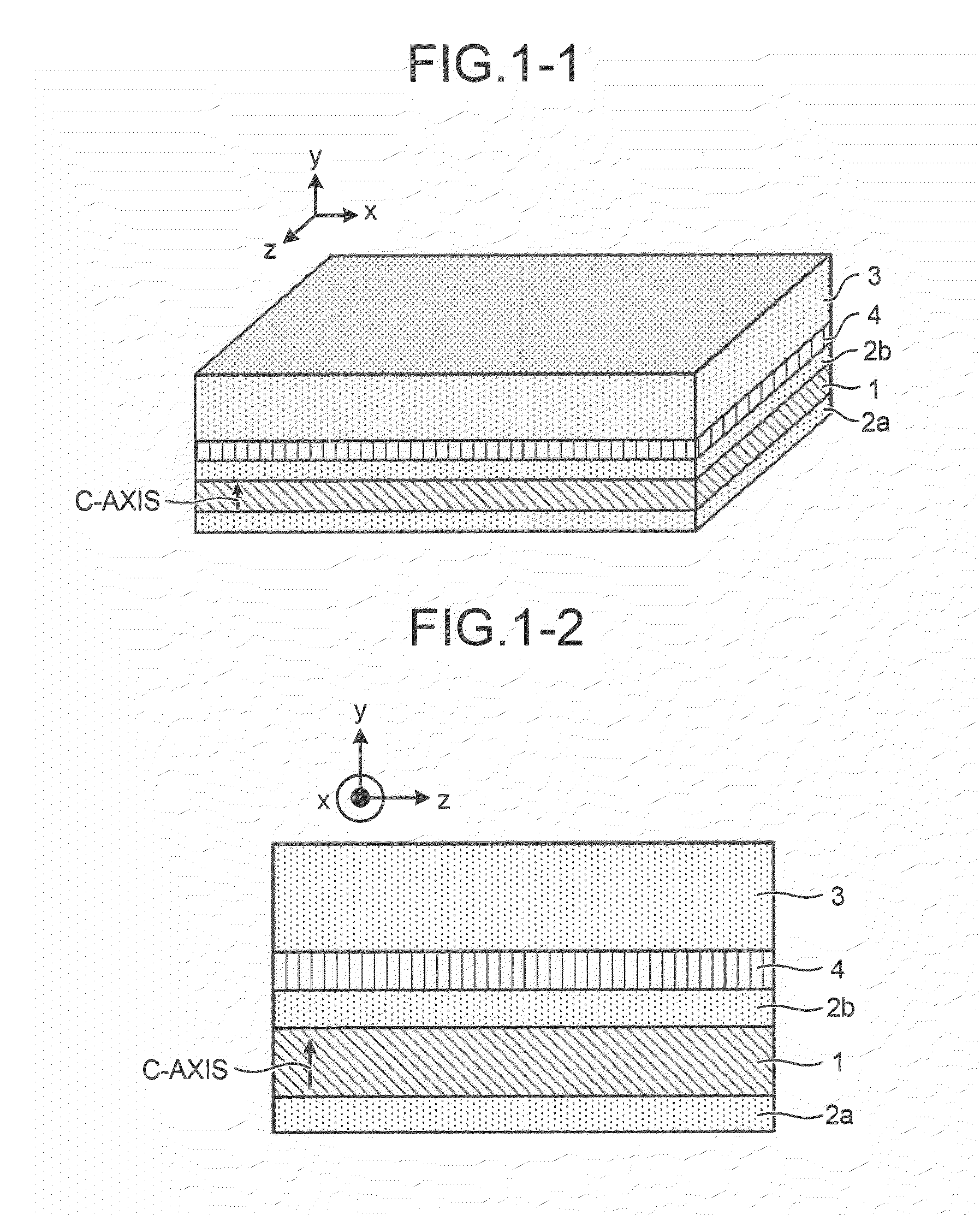
[0029]FIG. 1-1 is a schematic diagram showing a perspective view of a structure of a planar waveguide laser device according to a first embodiment of the present invention.

[0030]FIG. 1-2 is a schematic diagram showing a cross section of the structure of the planar waveguide laser device according to the first embodiment. The planar waveguide laser device includes a laser medium 1 having a plate-like shape and clad 2a and 2b provided on both the top and bottom surfaces of this laser medium 1. In addition, a substrate 3 is adhered to the outer surface of either one of the clad 2a and 2b (clad 2b in this example) by way of a bonding agent 4. In FIGS. 1-1 and 1-2, it is assumed that, in a plane parallel to the rectangular top and bottom surfaces having the largest area in the laser medium 1, directions parallel to two orthogonal sides of this plane are x-axis and z-axis and that a direction perpendicular to these two axes, the x-axis and the z-axis, is y-axis. Here, it is assumed that a...

second embodiment

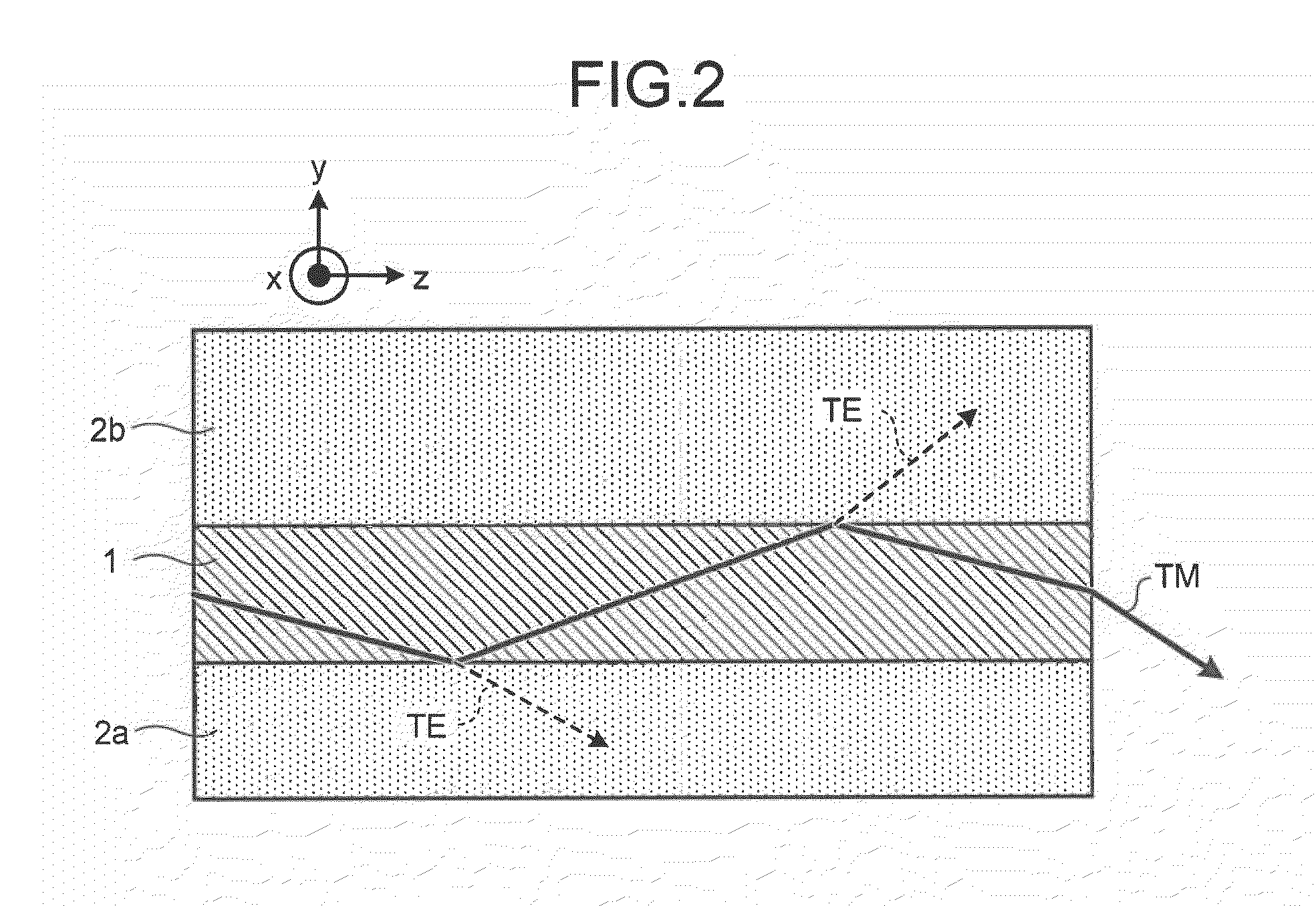
[0052]FIG. 4 is a schematic diagram showing examples of travelling paths of the laser light in the planar waveguide laser device according to the first embodiment. According to the first embodiment, if the refractive index of the outside of the clad 2a and 2b is smaller than the refractive index of the clad 2a and 2b, the laser light in the emission mode escaping into the clad 2a and 2b is reflected at the external boundary of the clad 2a and 2b, and comes back into the laser medium 1, where it is amplified (hereinafter, amplification of light that is not the laser light targeted for outputting is referred to as parasitic amplification), in addition to the laser light oscillated in the waveguide mode L1. This may cause a phenomenon in which the gain accumulated in the laser medium 1 is consumed. In such a situation, the laser light that is reflected at the boundary between the clad 2a and 2b and the outside is directly output through the output end surface, which is an out-of-clad p...


PUM


Abstract

A planar waveguide laser device forms a waveguide by a plate-like laser medium having birefringence and clad attached to at least one of the surfaces of the laser medium perpendicular to its thickness direction, amplifies laser light by a gain produced by excitation light incident on the laser medium, and performs laser oscillation. The laser medium is formed of a material having an optic axis on a cross section perpendicular to the light axis, which is the laser travelling direction. The clad is formed of a material having a refractive index in a range between refractive indexes of two polarized lights that travel along the light axis in the laser medium and have oscillation surfaces that are orthogonal to each other. The planar waveguide laser device readily oscillates linearly polarized laser light.

Description

TECHNICAL FIELD[0001]The present invention relates to a planar waveguide laser device having a planar waveguide structure that is suitable for a light source of a printer, a projection television, and the like.BACKGROUND ART[0002]A planar waveguide laser has a structure in which a thin, plate-like laser medium that extends in a laser light traveling direction is sandwiched from its top and bottom surfaces by a clad that has a lower refractive index than that of the laser medium. The structure causes the laser medium to function also as a waveguide. Because of its small waveguide thickness and high excitation density, the planar waveguide laser can attain a high gain even when a laser medium having a small cross section area for stimulated emission is adopted. This realizes an oscillation operation with a high degree of efficiency. Furthermore, by widening the waveguide in its width direction, scaling of the output can be realized while the excitation density is maintained at a prede...

Claims


Application Information

Patent Timeline
Patent Type & Authority Applications(United States)
IPC IPC(8): H01S5/327H01S5/10
CPCH01S3/0612H01S3/0625H01S3/0632H01S3/1673H01S3/1308H01S3/1611H01S3/10061
Inventor YANAGISAWA, TAKAYUKIHIRANO, YOSHIHITOYAMAMOTO, SHUHEIKOYATA, YASUHARU
Owner MITSUBISHI ELECTRIC CORP
Why Eureka
Try Eureka