Manufacturing method of light-emitting diode

a technology of light-emitting diodes and manufacturing methods, which is applied in the direction of basic electric elements, electrical apparatus, and semiconductor devices

Active Publication Date: 2010-07-29
CITIZEN ELECTRONICS CO LTD +1
View PDF1 Cites 38 Cited by
  • Summary
  • Abstract
  • Description
  • Claims
  • Application Information

AI Technical Summary

Benefits of technology

[0018]In the manufacturing method of LED in the present invention, the respective pairs of element electrodes positioned at second surfaces of the plurality of LED elements that are attached at their first surfaces onto the expanded enlarged expanding tape are collectively mounted on the respective pairs of the electrodes on the printed-circuit board assembly, and ther...

Problems solved by technology

There is thus a problem that, although dicing into individual LED elements 4 allows the plurality of LED elements 4 having the pair of electrode plates formed on the upper and lower surfaces (or right and left surfaces) to be obtained, the L...

Method used


Image

  • Manufacturing method of light-emitting diode
  • Manufacturing method of light-emitting diode
  • Manufacturing method of light-emitting diode

Examples


Embodiment Construction

[0043]Embodiments of a manufacturing method of an LED in accordance with the present invention are now described in detail with reference to the accompanying drawings.

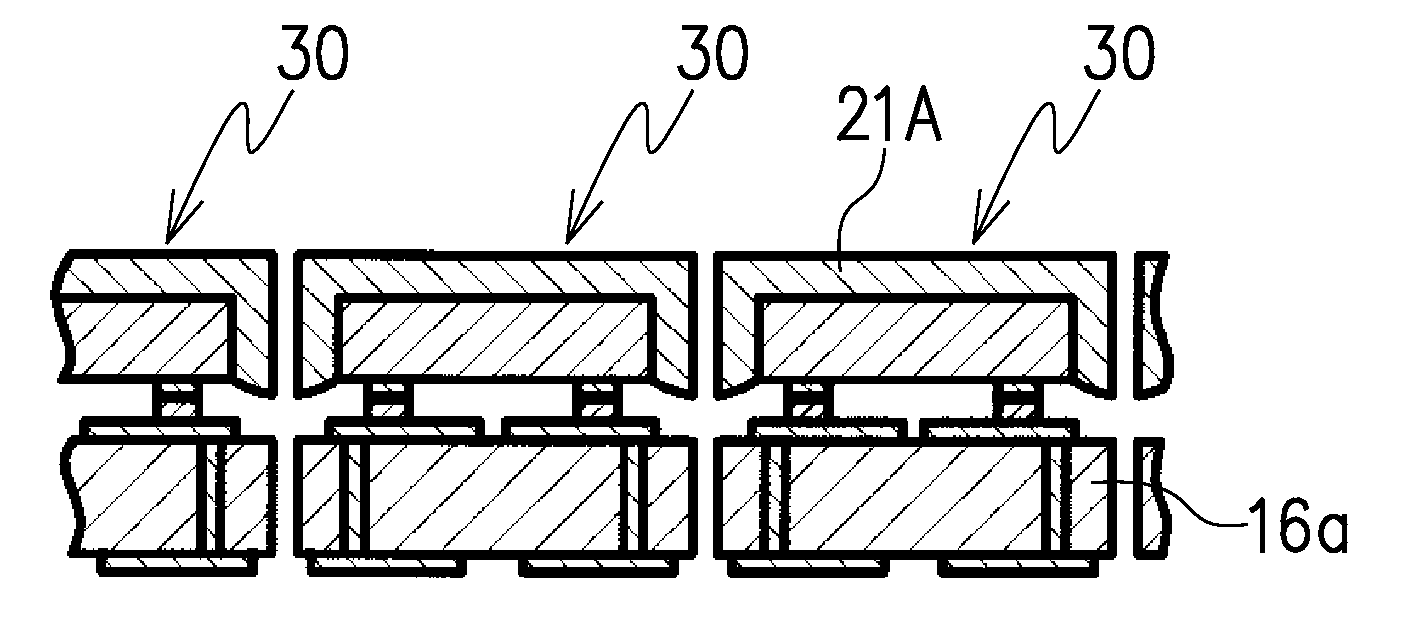
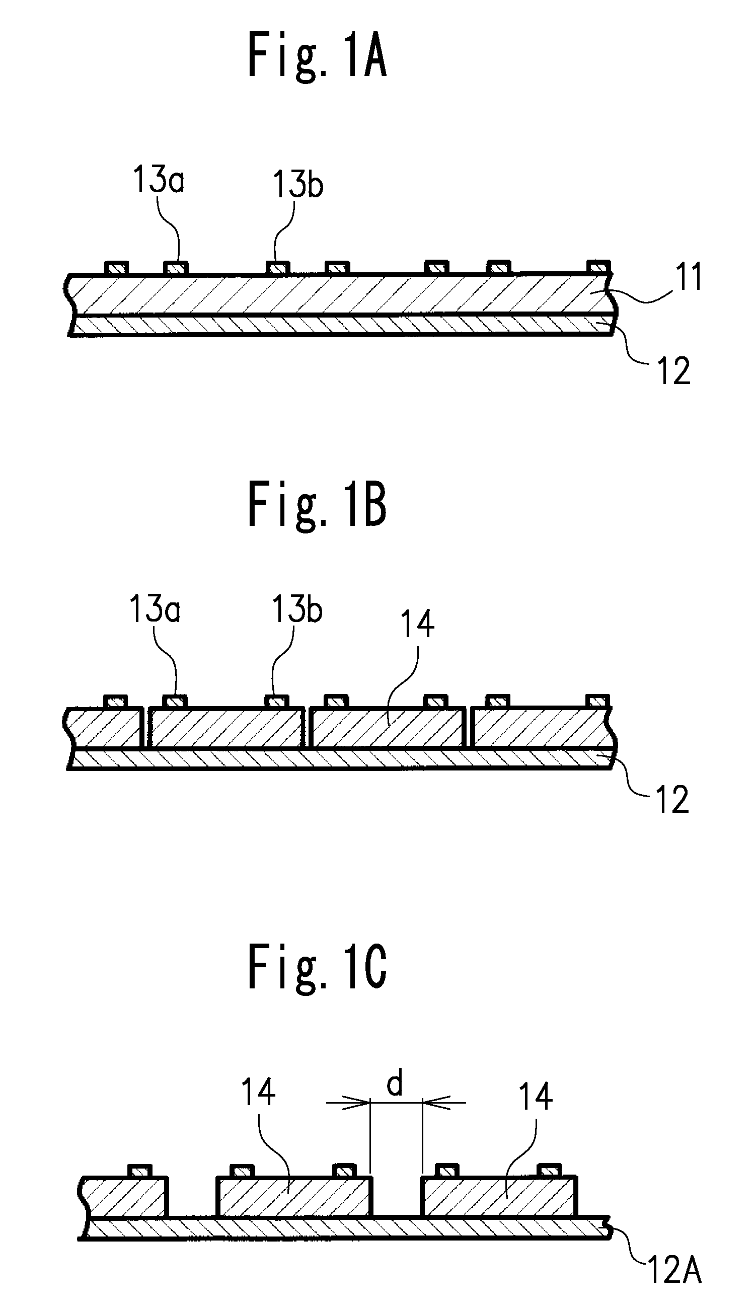
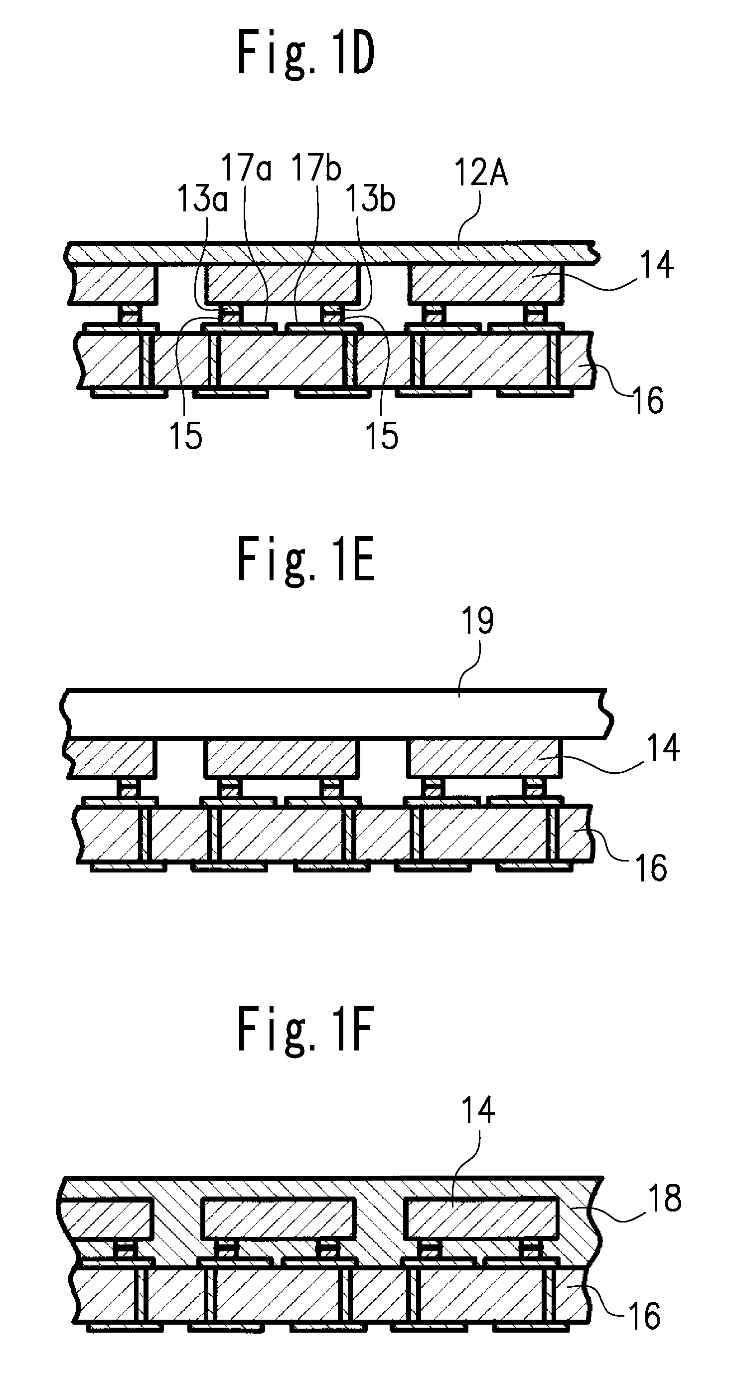
[0044]First, an embodiment of the manufacturing method of LED in the present invention is described. FIG. 2 shows an LED 20 in which an LED element 14 is mounted on the printed-circuit board 16a. For more details, anode and cathode element electrodes 13a and 13b that are formed at one surface of the LED element 14 are electrically connected through bumps 15 to a pair of electrodes 17a and 17b that are formed on the printed-circuit board 16a, respectively. The pair of electrodes 17a and 17b of the printed-circuit board 16a include a pair of upper electrodes formed on an upper surface of the printed-circuit board 16a and a pair of lower electrodes formed on a lower surface of the printed-circuit board 16a, and through-holes 22a and 22b that electrically connect the upper and lower electrodes, respectively. In addition, i...


PUM


Abstract

A manufacturing method of an LED comprises attaching an LED epitaxial wafer (LED wafer) to an expanding tape, dicing the LED wafer on the expanding tape longitudinally and laterally to a certain element size to divide into a plurality of LED elements, expanding the expanding tape to a certain size to form an enlarged expanding tape, placing respective pairs of element electrodes of the plurality of LED elements that are attached to the enlarged expanding tape on respective pairs of electrodes on a printed-circuit board assembly collectively to perform a bonding, and removing the enlarged expanding tape from the plurality of the LED elements.

Description

CROSS REFERENCE TO THE RELATED APPLICATION[0001]The application is based on and claims the priority benefit of Japanese Patent Application No. 2009-14913, filed on Jan. 27, 2009, the entire description of which is incorporated herein by reference.BACKGROUND OF THE INVENTION[0002]1. Field of the Invention[0003]The present invention relates to a manufacturing method of light-emitting diode, more specifically to a manufacturing method of a light-emitting diode in which a light-emitting diode element is mounted on a substrate.[0004]2. Description of the Related Art[0005]In recent years, there is developed a white light source comprising a blue light-emitting diode element and a fluorescent material that is excited by a portion of blue light emitted from the blue light-emitting diode element, and, as a result, a conventional light source in lighting, automobile lamps, TVs and personal computers is being rapidly replaced by a light-emitting diode (hereinafter referred to as “LED”). Variou...

Claims


Application Information

Patent Timeline
IPC IPC(8): H01L21/50
CPCH01L21/6836H01L2924/12041H01L24/13H01L24/81H01L24/97H01L33/005H01L33/486H01L33/54H01L33/62H01L2221/68336H01L2221/68354H01L2221/68377H01L2224/16H01L2224/81205H01L2224/81801H01L2224/97H01L2924/01015H01L2924/01075H01L2924/01079H01L2924/01082H01L2924/01322H01L2933/0041H01L24/11H01L2924/01033H01L2924/01006H01L2224/81H01L2224/05573H01L2224/05568H01L2924/00014H01L2224/0554H01L2224/05599H01L2224/0555H01L2224/0556
Inventor HORIUCHI, MEGUMI
Owner CITIZEN ELECTRONICS CO LTD
Why Eureka
Try Eureka