Routing Method for Double Patterning Design

Active Publication Date: 2010-08-05
TAIWAN SEMICON MFG CO LTD
View PDF9 Cites 53 Cited by
  • Summary
  • Abstract
  • Description
  • Claims
  • Application Information

AI Technical Summary

Benefits of technology

[0007]The advantageous features of the present invention include reduced design effort for solving rule violations

Problems solved by technology

With the increasing down-scaling of integrated circuits, optical proximity effect posts an increasingly greater problem.
When two separate features are too close to each other, the optical proximity effect may cause the features to short to each other.
When the double patterning technology is used in the formation of metal layers, which are used to rou

Method used


Image

  • Routing Method for Double Patterning Design
  • Routing Method for Double Patterning Design
  • Routing Method for Double Patterning Design

Examples


Embodiment Construction

[0016]The making and using of the embodiments are discussed in detail below. It should be appreciated, however, that the embodiments provide many applicable inventive concepts that can be embodied in a wide variety of specific contexts. The specific embodiments discussed are merely illustrative of specific ways to make and use the invention, and do not limit the scope of the invention.

[0017]A novel double patterning routing method, a router framework, and the resulting double patterning mask sets are presented. The variations of the embodiment are then discussed. Throughout the various views and illustrative embodiments, like reference numbers are used to designate like elements.

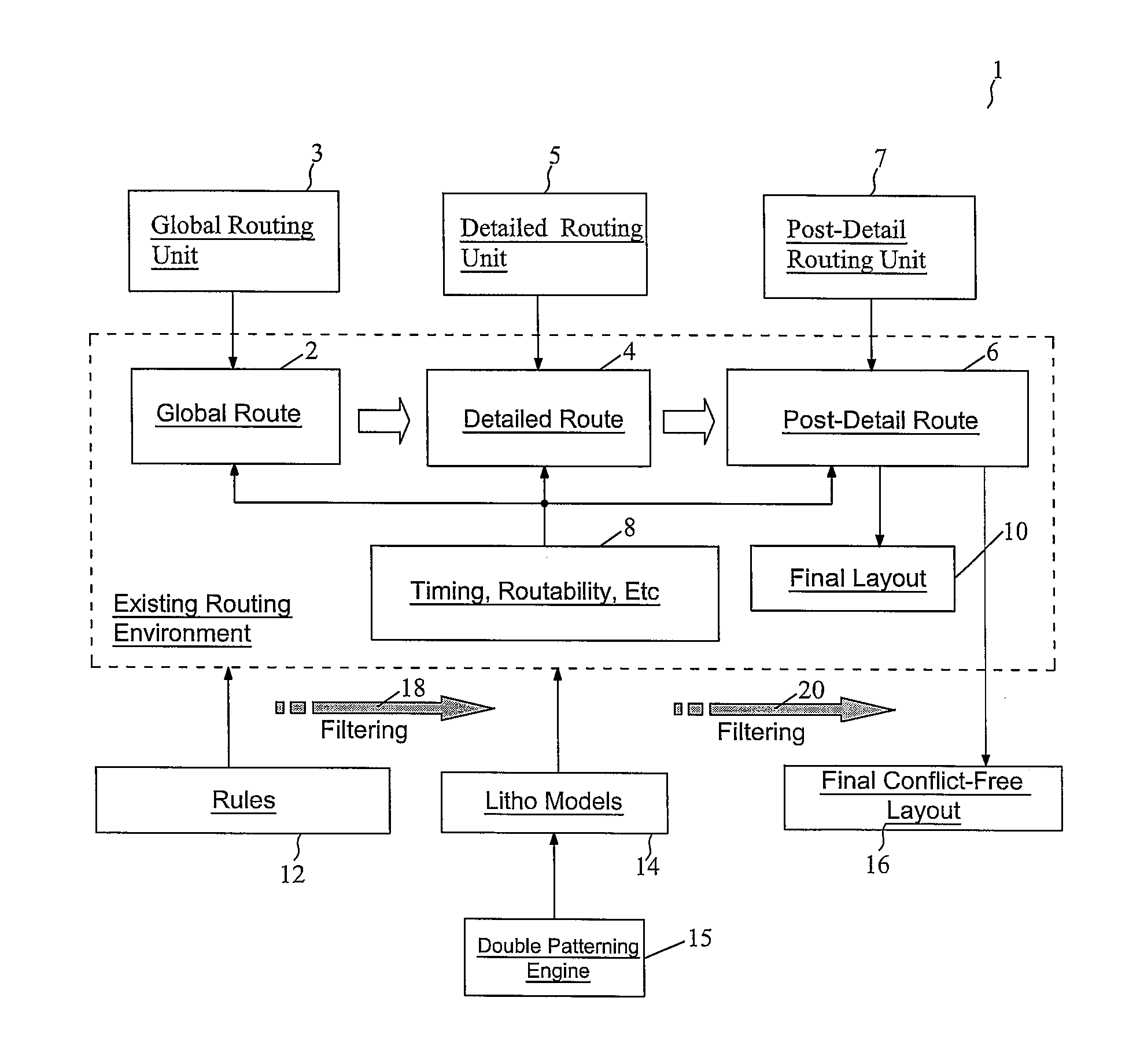
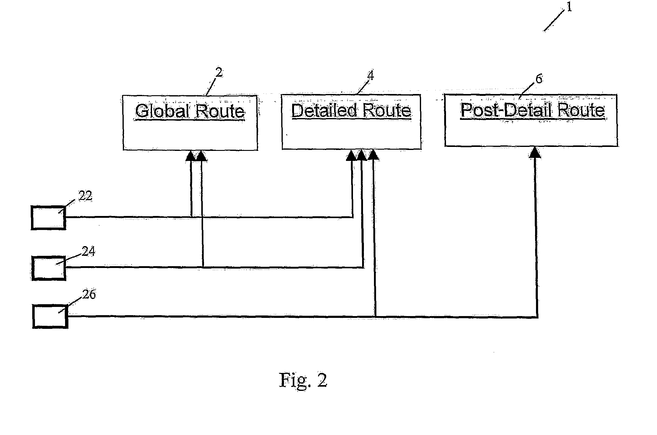
[0018]FIG. 1 schematically illustrates a block diagram of router framework 1, which includes double patterning lithography models (Litho models 14). Router framework 1 may perform three types of routing tasks, global route (step 2), detailed route (step 4), and post-detail route (step 6), which may be perfor...


PUM


Abstract

A method of designing a double patterning mask set includes dividing a chip into a grid comprising grid cells; and laying out a metal layer of the chip. In substantially each of the grid cells, all left-boundary patterns of the metal layer are assigned with a first one of a first indicator and a second indicator, and all right-boundary patterns of the metal layer are assigned with a second one of the first indicator and the second indicator. Starting from one of the grid cells in a row, indicator changes are propagated throughout the row. All patterns in the grid cells are transferred to the double patterning mask set, with all patterns assigned with the first indicator transferred to a first mask of the double patterning mask set, and all patterns assigned with the second indicator transferred to a second mask of the double patterning mask set.

Description

[0001]This application claims the benefit of U.S. Provisional Application No. 61 / 149,637 filed on Feb. 3, 2009, entitled “Routing Method for Double Patterning Design,” which application is hereby incorporated herein by reference.TECHNICAL FIELD[0002]This invention relates generally to integrated circuit manufacturing processes, and more particularly to using double patterning technology to reduce the lithography limits of integrated circuits, and even more particularly metal routing using the double patterning technology.BACKGROUND[0003]Double patterning is a technology developed for lithography to enhance the feature density. Typically, for forming features of integrated circuits on wafers, lithography technology is used, which involves applying a photo resist, and defining patterns on the photo resist. The patterns in the patterned photo resist are first defined in a lithography mask, and are defined either by the transparent portions or by the opaque portions in the lithography m...

Claims


Application Information

Patent Timeline
IPC IPC(8): G06F17/50
CPCG03F1/14G03F1/144G03F7/70433G06F2217/12G03F7/705G06F17/5077G03F7/70466G03F1/00G06F2119/18G06F30/394Y02P90/02
Inventor CHENG, YI-KANLU, LEE-CHUNGLIU, RU-GUNLAI, CHIH-MING
Owner TAIWAN SEMICON MFG CO LTD
Why Eureka
Try Eureka