Memory interface and operation method of it

a memory interface and operation method technology, applied in the direction of information storage, static storage, digital storage, etc., can solve the problems of difficult to determine whether the cause is caused, the logical state of ddr2 sdram and ddr3 sdram is unstable, and the conventional memory interface cannot read normal data in read

Active Publication Date: 2010-08-12
RENESAS ELECTRONICS CORP
View PDF1 Cites 21 Cited by
  • Summary
  • Abstract
  • Description
  • Claims
  • Application Information

AI Technical Summary

Benefits of technology

[0020]According to the present invention, in a memory system for reading and writing data by using a data strobe signal, a technique of properly performing timing calibration in an initialization sequence can be provided.

Problems solved by technology

The commercially available semiconductor storage devices such as DDR2 SDRAM and DDR3 SDRAM have unstable logical states of internal circuits immediately after power-on.
When data cannot be correctly read in read, it is difficult to determine whether it is caused due to failure of initial write or a problem in the read.
As described above, when the timing calibration is performed, when first write cannot be reliably performed, the conventional memory interface cannot read normal data in read.
For this reason, in the conventional memory interface, when data cannot be completely read in the read, it is difficult to determine whether the failure is due to failure of the first write, failure of fetching of data or a problem in the read in spite of success of the first write.

Method used


Image

  • Memory interface and operation method of it
  • Memory interface and operation method of it
  • Memory interface and operation method of it

Examples


Embodiment Construction

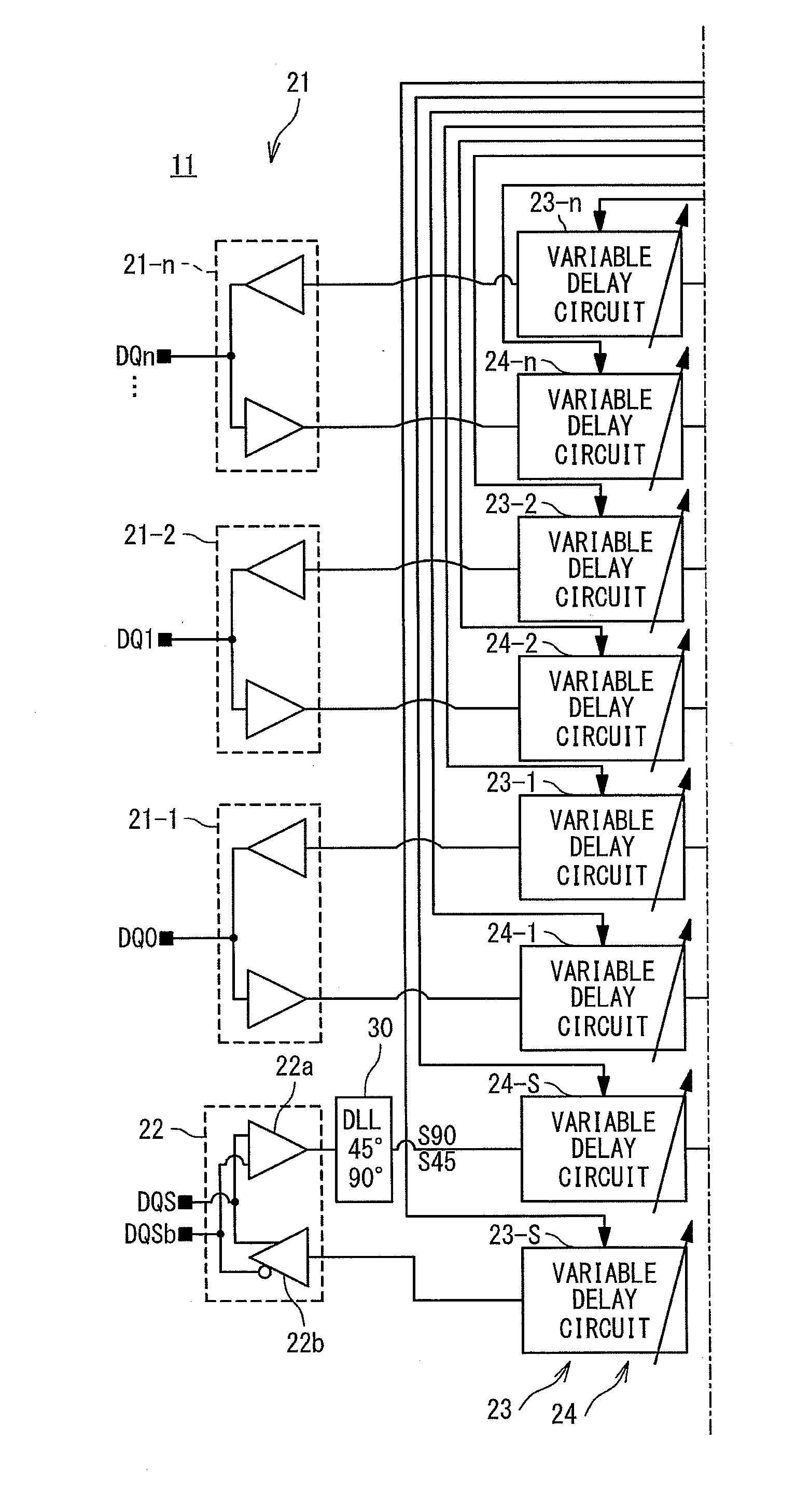
[0032]Hereinafter, a memory interface 11 according to the present invention will be described with reference to the attached drawings. The memory interface 11 according to an embodiment of the present invention controls read / write of data from / to a semiconductor memory device in response to a data strobe signal. The memory interface 11 in the present embodiment can be applied to any equipment without limitation, and the semiconductor memory device mounted in the equipment may respond to the data strobe signal. Accordingly, a configuration and an operation of the present embodiment will be described below using a case where the memory interface 11 is mounted in a computer system 1 as an example. In the drawings for showing the configuration and the operation of the present embodiment, the same reference numerals are assigned to the same components.

[0033]FIG. 3 is a block diagram showing a configuration of the computer system 1 mounted with the memory interface 11 in the present embod...


PUM


Abstract

A memory interface includes a first delaying circuit configured to delay write data to be supplied to an input buffer; a second delaying circuit configured to delay read data read out from an output buffer; a data write circuit configured to supply said write data to a memory through said first delaying circuit; and a data read circuit configured to read said write data written in said memory, as said read data through said second delaying circuit. A control circuit is configured to detect positions of a start edge and end edge of an eye opening which is formed based on fluctuation of said write data or said read data, to specify an intermediate position of the start edge and the end edge, and to determine a phase of a data strobe signal based on a difference between the intermediate position and one of the start edge and the end edge.

Description

INCORPORATION BY REFERENCE[0001]This patent application claims a priority on convention based on Japanese Patent Application No. 2008-253989. The disclosure thereof is incorporated herein by reference.BACKGROUND OF THE INVENTION[0002]1. Field of the Invention[0003]The present invention relates to a memory interface and an operation method of the memory interface.[0004]2. Description of Related Art[0005]With advancement of information processing technique, a semiconductor memory device is possible to perform a high speed operation with less consumed power. As such a semiconductor memory device, a technique is known which uses a data strobe signal (DQS). The semiconductor memory devices are exemplified by semiconductor storage devices having a data transfer rate in a Gbps order such as DDR2 (Double Data Rate 2) SDRAM (Synchronous DRAM) and DDR3 SDRAM.[0006]Generally, a memory interface is interposed between a high-speed semiconductor memory device and a central processing unit (CPU). ...

Claims


Application Information

Patent Timeline
Patent Type & Authority Applications(United States)
IPC IPC(8): G11C7/00
CPCG11C7/1006G11C7/1051G11C7/1066G11C7/1069G11C7/1078G11C7/1093G11C29/028G11C7/22G11C7/222G11C29/02G11C29/022G11C29/023G11C7/1096
Inventor KUROKI, REIKO
Owner RENESAS ELECTRONICS CORP
Why Eureka
Try Eureka