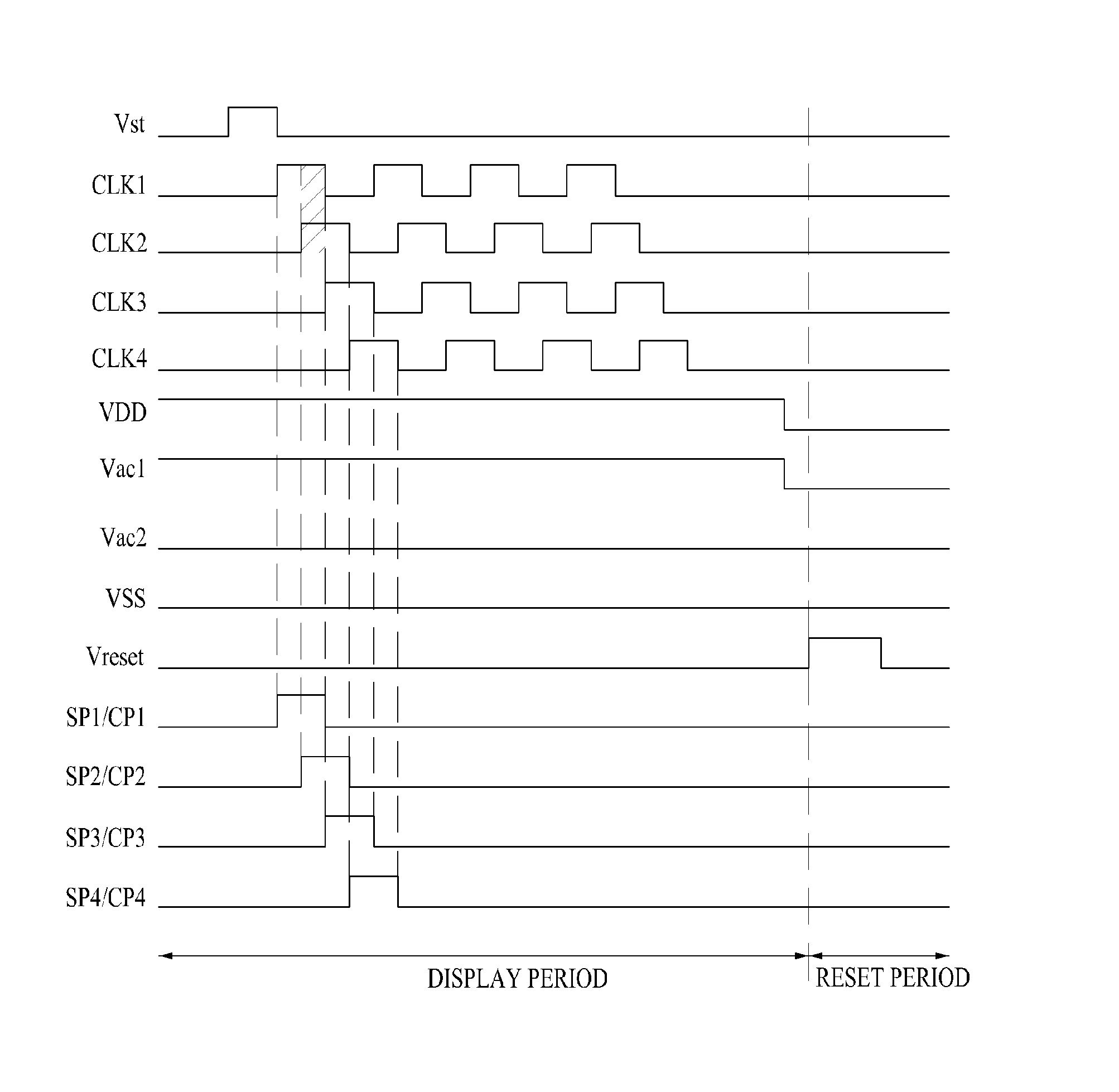
Shift register

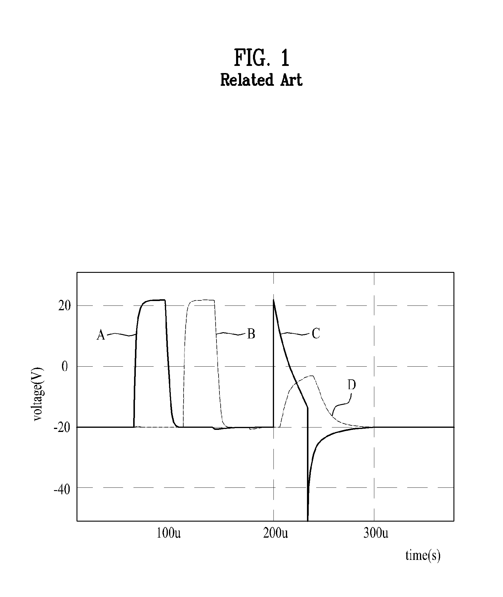
a technology of shift register and shift voltage, applied in the field of shift register, can solve the problems of picture quality degradation, downstream stage may be set or upstream stage may be reset with undesired timings, etc., and achieve the effect of rapid discharging of spike voltag

Active Publication Date: 2010-08-26
E INK CORPORATION
View PDF4 Cites 42 Cited by
  • Summary
  • Abstract
  • Description
  • Claims
  • Application Information

AI Technical Summary

Benefits of technology

[0009]An object of the present invention is to provide a shift register which is not influenced by a spike voltage and has a discharging unit capable of rapidly discharging the spike voltage.

Problems solved by technology

Accordingly, for the one frame period, the gate line may be driven more than once and, thus, the thin film transistor may be turned on more than once, thereby causing a wrong data voltage to be supplied to the pixel, resulting in degradation in picture quality.
A more serious problem is that a downstream stage may be set or an upstream stage may be reset with undesired timings because this spike voltage may be spread to the downstream stage and upstream stage along this gate line.
The above problem more frequently occurs particularly in an Electrophoretic Display (EPD) which displays an image by moving black pigment particles and white pigment particles vertically using a field effect.

Method used


Image

  • Shift register
  • Shift register
  • Shift register

Examples


first embodiment

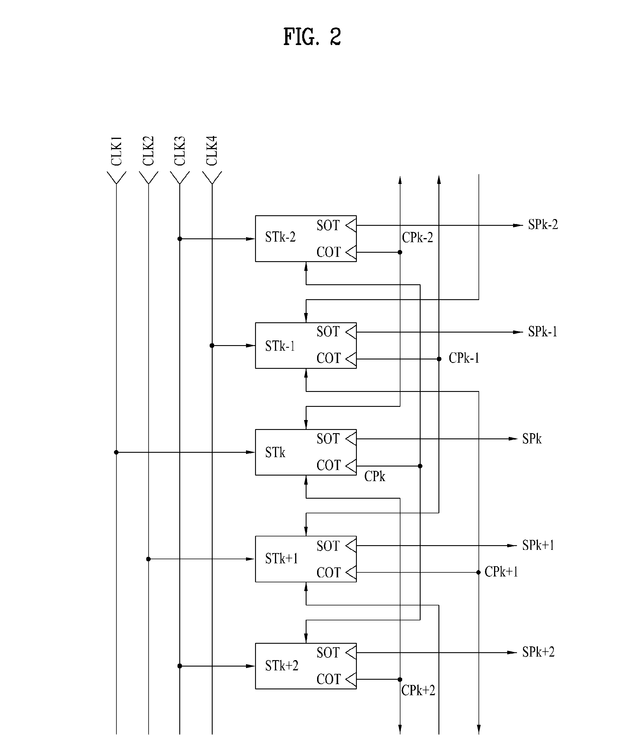
[0044]FIG. 3 is a block diagram showing the configuration of any one of the stages of FIG. 2.

[0045]Each stage includes, as shown in FIG. 3, a scan pulse output unit SO controlled according to voltages at a set node Q and reset node QB for outputting a scan pulse and supplying it to a corresponding gate line through the scan output terminal SOT, a carry pulse output unit CO controlled according to the voltages at the set node Q and reset node QB for outputting a carry pulse and supplying it to an upstream stage and a downstream stage through the carry output terminal COT, a node controller NC for controlling the voltage states of the set node Q and reset node QB in response to a carry pulse from the upstream stage and a carry pulse from the downstream stage, and a discharging unit 300 connected to any one of a plurality of clock transfer lines which transfer a plurality of clock pulses with different phases, respectively, and the scan output terminal SOT for discharging a spike volta...

second embodiment

[0086]FIG. 6 is a block diagram showing the configuration of any one of the stages of FIG. 2.

[0087]Each stage includes, as shown in FIG. 6, a scan pulse output unit SO controlled according to voltages at a set node Q, first reset node QB1 and second reset node QB2 for outputting a scan pulse and supplying it to a corresponding gate line through the scan output terminal SOT, a carry pulse output unit CO controlled according to the voltages at the set node Q, first reset node QB1 and second reset node QB2 for outputting a carry pulse and supplying it to an upstream stage and a downstream stage through the carry output terminal COT, a node controller NC for controlling the voltage states of the set node Q, first reset node QB1 and second reset node QB2 in response to a carry pulse from the upstream stage and a carry pulse from the downstream stage, and a discharging unit 300 connected to any one of a plurality of clock transfer lines which transfer a plurality of clock pulses with diff...


PUM


Abstract

A shift register which is capable of minimizing a spike voltage is disclosed. The shift register includes a plurality of stages, each including a plurality of nodes, a scan pulse output unit controlled according to voltages at the nodes for outputting a scan pulse and supplying it to a corresponding gate line through a scan output terminal, a carry pulse output unit controlled according to the voltages at the nodes for outputting a carry pulse and supplying it to an upstream stage and a downstream stage through a carry output terminal, a node controller for controlling voltage states of the nodes in response to a carry pulse from the upstream stage and a carry pulse from the downstream stage, and a discharging unit connected to any one of a plurality of clock transfer lines and the scan output terminal for discharging a spike voltage of the scan output terminal.

Description

[0001]This application claims the benefit of Korean Patent Application No. 10-2009-0015644 filed on Feb. 25, 2009, which is hereby incorporated by reference as if fully set forth herein.BACKGROUND OF THE INVENTION[0002]1. Field of the Invention[0003]The present invention relates to a shift register, and more particularly, to a shift register which is capable of preventing degradation in picture quality of a display device resulting from a spike voltage.[0004]2. Discussion of the Related Art[0005]In order to sequentially drive gate lines of a display device, there is a need for a shift register to supply scan pulses to the gate lines in order. The shift register includes a plurality of stages for outputting the scan pulses, respectively. The output terminal of each stage is connected one-to-one to a corresponding one of the gate lines. Each gate line is connected to corresponding pixels of the display device. In detail, each pixel includes a thin film transistor which is turned on in...

Claims


Application Information

Patent Timeline
Patent Type & Authority Applications(United States)
IPC IPC(8): G06F3/038
CPCG09G3/344G11C19/28G09G2330/04G09G2310/0267G09G3/20H03K19/00G11C27/04
Inventor KIM, BINNJANG, YONG-HO
Owner E INK CORPORATION
Why Eureka
Try Eureka