Method for the fabrication of semiconductor integrated circuit device

a semiconductor integrated circuit and integrated circuit technology, applied in the direction of semiconductor devices, electrical equipment, transistors, etc., can solve the problems of cross contamination, difficult to provide individual immersion-type exposure apparatuses for individual steps, high operating costs, etc., and achieve the effect of low running costs

Inactive Publication Date: 2010-09-09
RENESAS ELECTRONICS CORP
View PDF4 Cites 25 Cited by
  • Summary
  • Abstract
  • Description
  • Claims
  • Application Information

AI Technical Summary

Benefits of technology

[0015]Accordingly, an object of the present invention is to provide a process for fabricating a semiconductor integrated circuit device with high reliability.
[0021]Specifically, the wet cleaning process of the wafer back side herein includes the two steps of carrying out a FPM process and carrying out a SPM process in this order and is performed before the lithography step. The wet cleaning process thereby remarkably reduces the heavy metal contaminants level of the wafer back side and prevents cross contamination through the lithography step.

Problems solved by technology

The immersion type exposure apparatus is very expensive, and it may be difficult to provide individual immersion type exposure apparatus for individual steps.
This may cause cross contamination typically from the back side of the previously passing wafer.
However, common techniques for the cleaning typically of back sides of wafers may not sufficiently effectively clean the above-mentioned back side containing a polysilicon as a main component.

Method used


Image

  • Method for the fabrication of semiconductor integrated circuit device
  • Method for the fabrication of semiconductor integrated circuit device
  • Method for the fabrication of semiconductor integrated circuit device

Examples


Embodiment Construction

Summary of Some Embodiments

[0044]Initially, representative embodiments of the present invention will be briefly illustrated below.

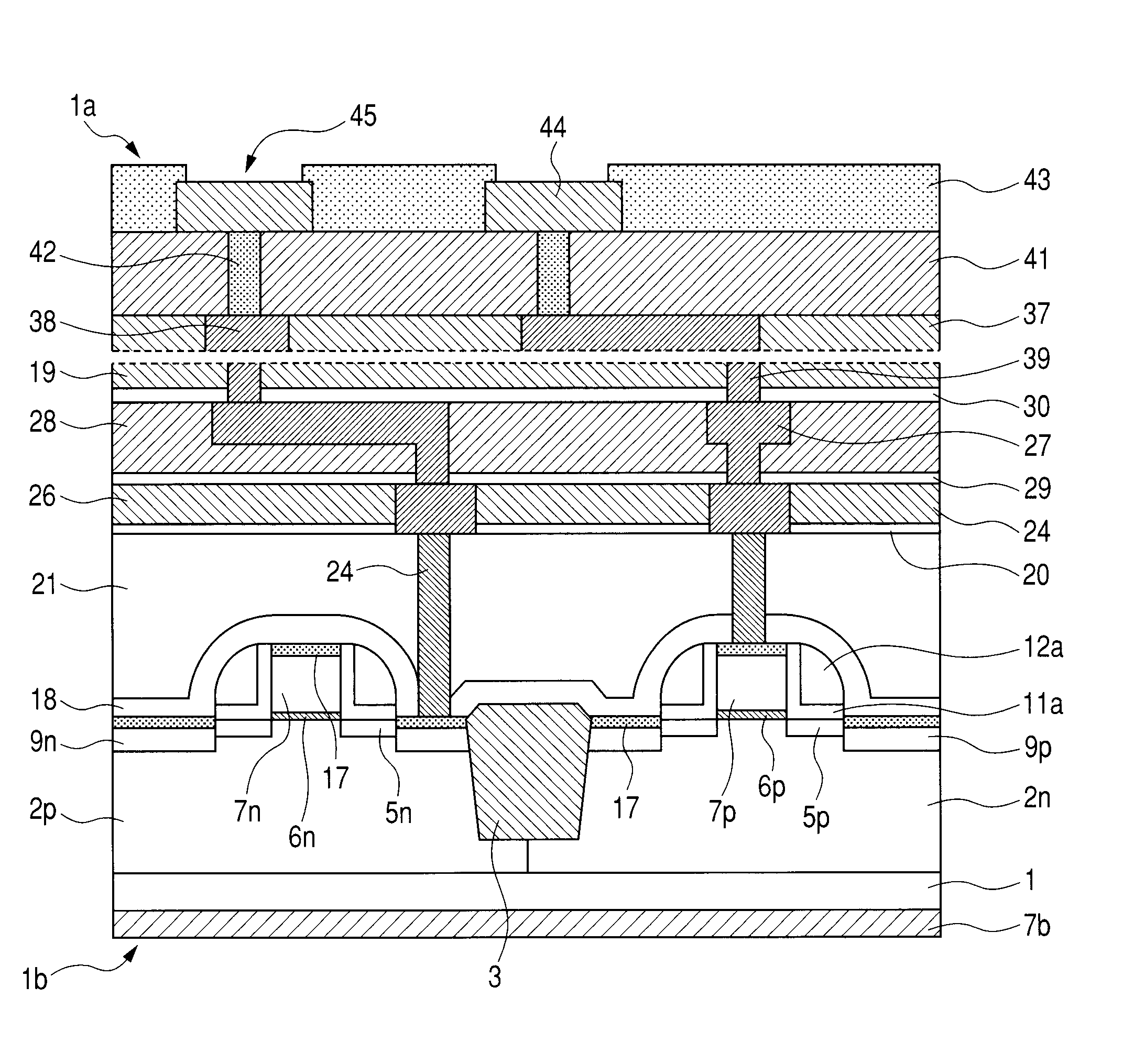
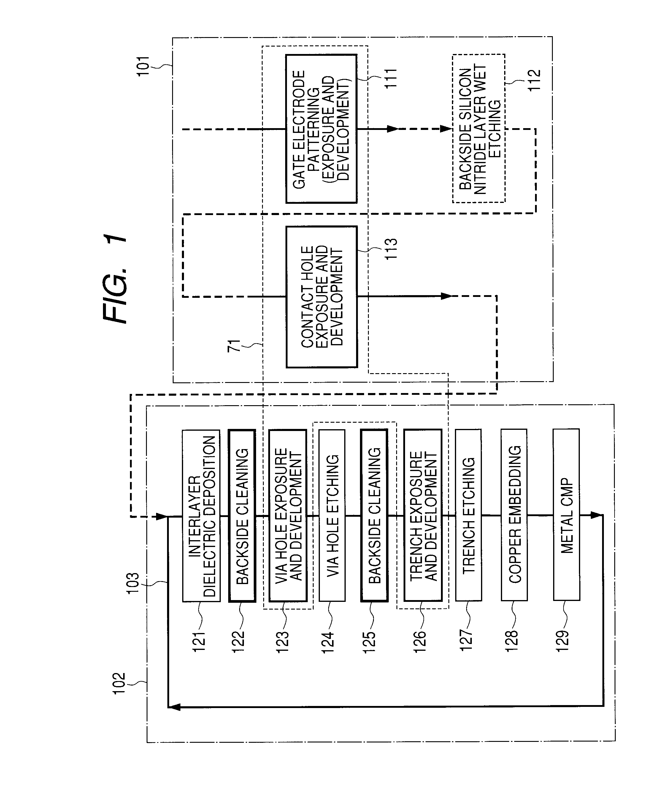
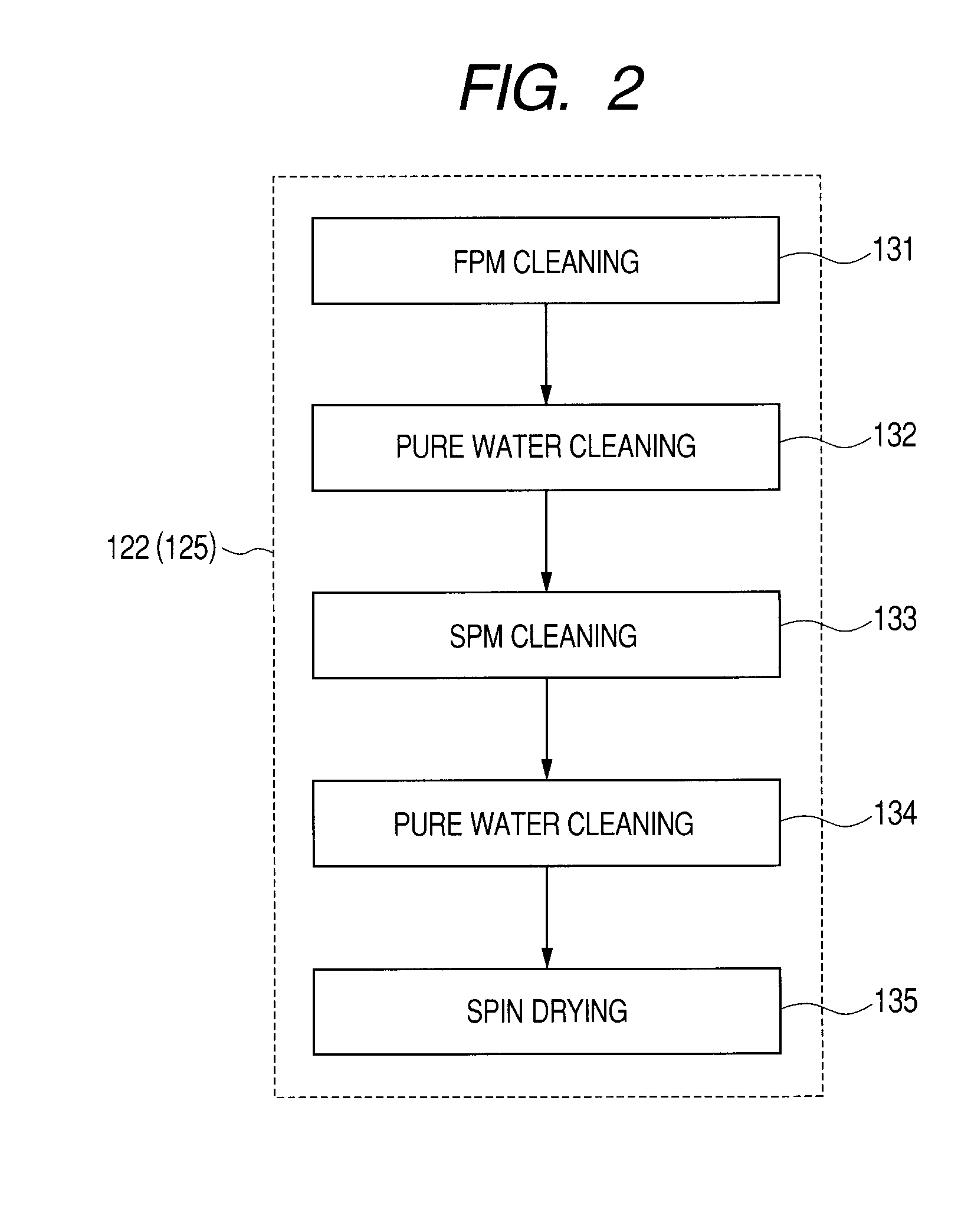
[0045]1. A method for fabricating a semiconductor integrated circuit device, comprising the steps of: (a) forming a second insulating film over a first insulating film over a device side of a wafer, the second insulating film to be an interlayer insulating film for an embedded wiring (for a buried interconnection); (b) after the step (a), carrying out a first wet cleaning of a back side of the wafer; (c) after the step (b), introducing the wafer into a first lithographic apparatus and carrying out a patterning of a first resist film; and (d) after the step (c), carrying out a first processing of the second insulating film by a first dry etching on the device side of the wafer in the presence of the patterned first resist film, in which the step (b) includes the substeps of: (b1) carrying out the first wet cleaning with a first aqueous solution containing ...


PUM

PropertyMeasurementUnit
temperaturesaaaaaaaaaa
wavelengthaaaaaaaaaa
timeaaaaaaaaaa

Abstract

In fabrication processes of semiconductor integrated circuit devices, a technique for improving the carrier mobility has been frequently employed. This technique utilizes strain caused by the stress typically of a silicon nitride film. With this, a batchwise wet processing with hot phosphoric acid should be performed so as to highly selectively remove the silicon nitride film over a complicated device structure on a front side of a wafer. This processing removes also a silicon nitride film on the back side of the wafer, and after a series of strain-imparting processes, a polysilicon member is exposed from the back side surface of the wafer. However, common techniques for cleaning typically of back sides of wafers may not sufficiently effectively clean the back side containing a polysilicon as a main component, because these techniques are designed to be adopted to a back side containing, for example, a silicon nitride film, but the polysilicon and the silicon nitride film differ from each other in properties. To void the problem, a wet cleaning process is performed before a lithography process. The wet cleaning process includes two steps, in which FPM cleaning and SPM cleaning are performed in this order.

Description

CROSS-REFERENCE TO RELATED APPLICATIONS[0001]The disclosure of Japanese Patent Application No. 2009-51666 filed on Mar. 5, 2009 including the specification, drawings and abstract is incorporated herein by reference in its entirety.BACKGROUND OF THE INVENTION[0002]The present invention relates to a technique that is effectively adopted so as to prevent heavy metal in fabrication methods for semiconductor integrated circuit devices (or semiconductor devices).[0003]Japanese Unexamined Patent Publication No. 2001-110766 or the corresponding U.S. Pat. No. 6,592,677 discloses a technique of carrying out a back-side cleaning of a silicon-based wafer after copper plating in a process for forming an embedded copper wiring. According to this technique, hydrophilicity is imparted to the back side of the wafer by cleaning the back side with a hydrofluoric acid-hydrogen peroxide aqueous solution (FPM) to remove a silicon oxide film together with contaminated metals such as copper from the back s...

Claims


Application Information

Patent Timeline
Patent Type & Authority Applications(United States)
IPC IPC(8): H01L21/30H01L21/28
CPCH01L21/02057H01L21/0209H01L21/31111H01L21/823807H01L29/6659H01L2924/0002H01L29/7833H01L29/7847H01L2924/00
Inventor OCHI, HIRONORI
Owner RENESAS ELECTRONICS CORP
Why Eureka
Try Eureka