Semiconductor memory device

Inactive Publication Date: 2010-09-16
KK TOSHIBA
View PDF5 Cites 17 Cited by
  • Summary
  • Abstract
  • Description
  • Claims
  • Application Information

AI Technical Summary

Benefits of technology

[0011]According to a first aspect of the present invention, there is provided a semiconductor memory device which includes a plurality of blocks each having a plurality of memory cells and in which data is erased in a unit of the block, the device comprising: a first storage region which has a plurality of blocks and in which first conversion from a logical address to a physical address is performed and data is written into a region specified by the physical address converted based on the first conversion; a second storage region which has a plurality of blocks and in which second conversion from a logical address to a physical address, the second conversion being different from the first conversion, is performed and d

Problems solved by technology

In the USB flash memory, an influence of overhead for the write performance involved in the data move increases as the physical block size becomes larger, obtaining the random write performance required by the Readyboost may possibly become difficult.

Method used


Image

  • Semiconductor memory device
  • Semiconductor memory device
  • Semiconductor memory device

Examples


first embodiment

[0021]A USB flash memory according to a first embodiment of the present invention will be first described.

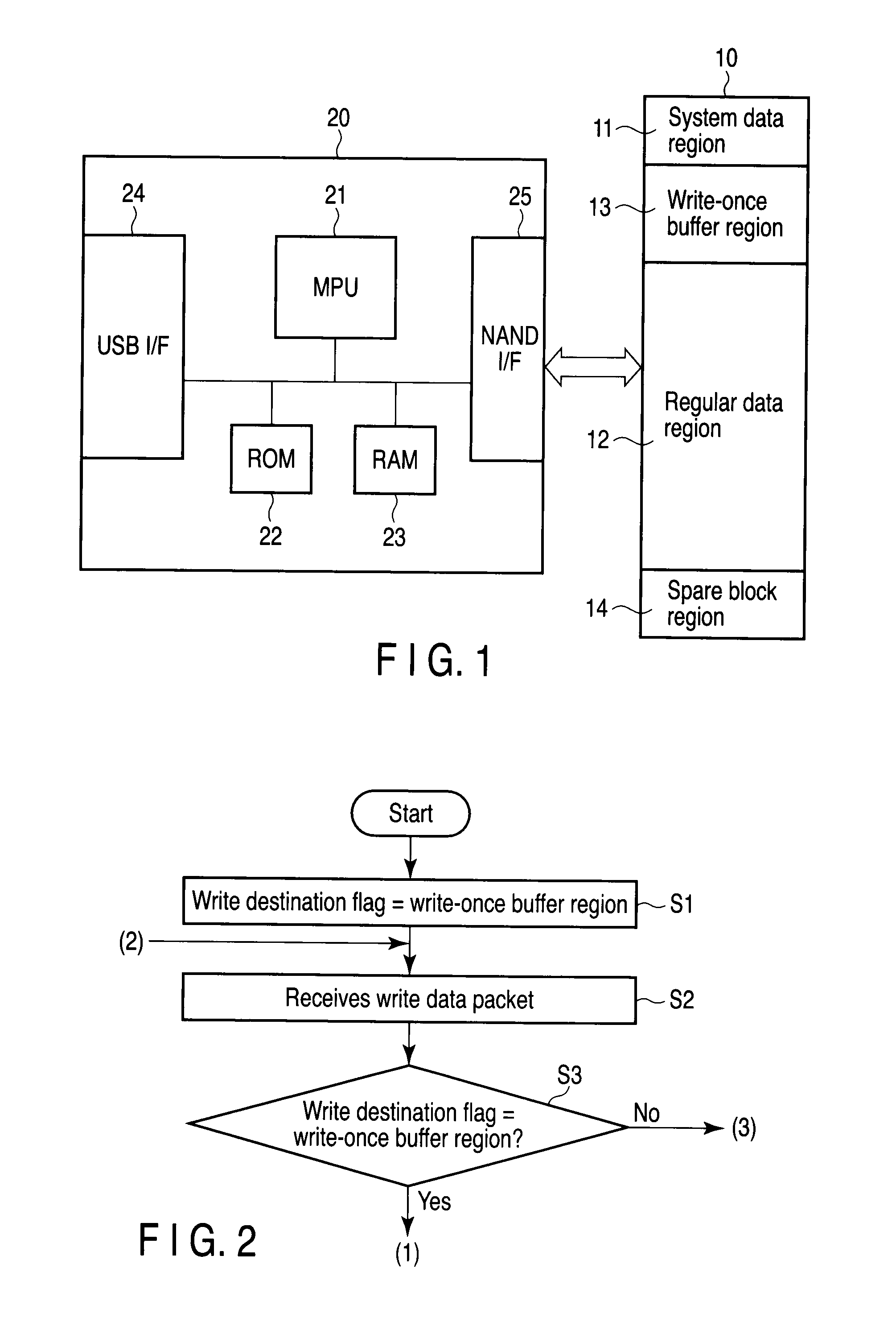
[0022]FIG. 1 is a block diagram showing a configuration of the USB flash memory according to the first embodiment. The USB flash memory has an NAND flash memory 10 and a controller 20 that controls operations of this NAND flash memory. The NAND flash memory 10 includes a plurality of blocks (logical blocks) each having a plurality of memory cells, and data is erased in a unit of the block. A block size (a storage capacity of the block) is, e.g., 1 MB or 1.5 MB.

[0023]The respective blocks of the NAND flash memory 10 are classified into a system data region 11 which stores a logical / physical conversion table or controller control information, a regular data region 12 which stores regular data, and a write-once buffer region 13 which is used to perform the random write at a high speed. Besides, there is also a spare block region 14 which is used for data move or replacement of a de...

second embodiment

[0047]A USB flash memory according to a second embodiment of the present invention will now be described. The second embodiment is different from the first embodiment in a write operation (an algorithm). A hardware configuration is the same as that of the first embodiment depicted in FIG. 1.

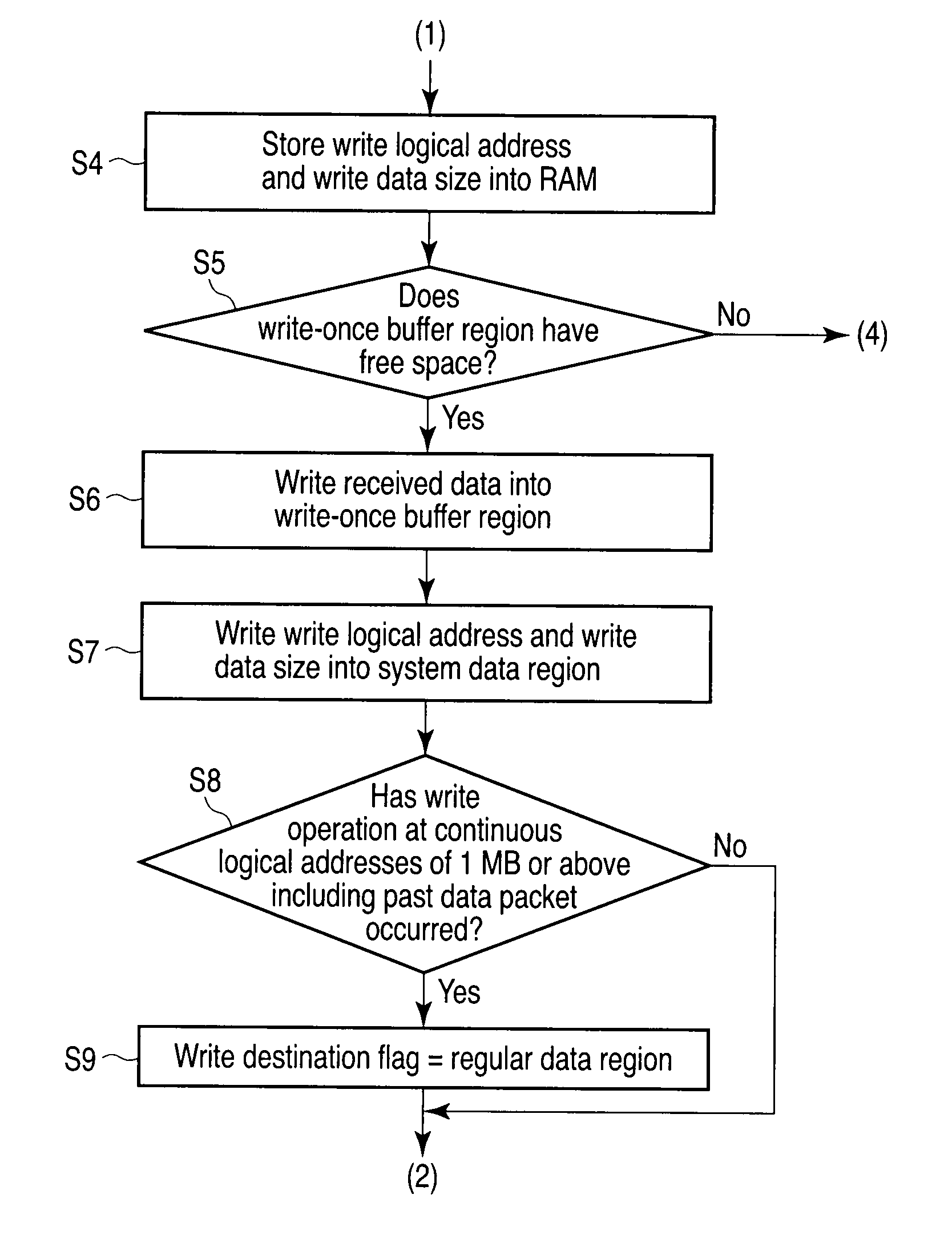
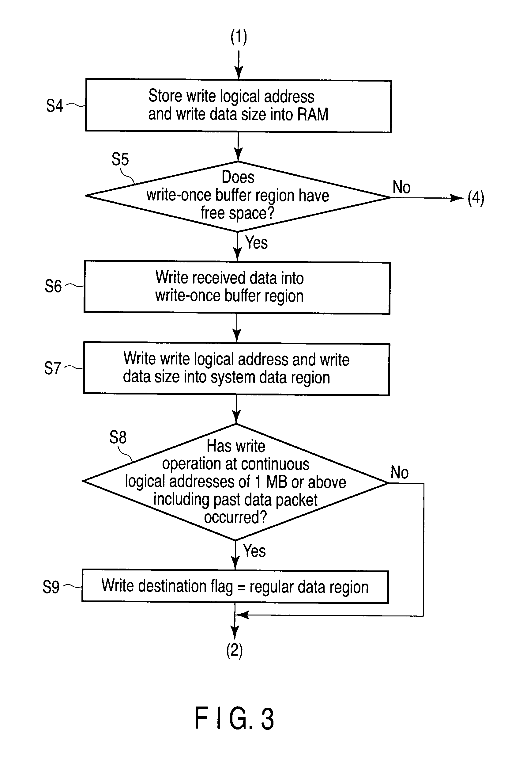
[0048]FIGS. 2, 3, and 8 are flowcharts showing a data write operation in a USB flash memory according to the second embodiment. In this embodiment, at a step S16, a condition that “after start of a write operation in units of 512 KB” is added as a condition to shift to a “write-once buffer write mode” at a step S12. Others are the same as those in the first embodiment.

[0049]In more detail, when a “write destination flag” is not set to a write-once buffer region 13 at a step S3, the control advances to a step S10. At the step S10, a write logical address and a write data size of write data are stored in an RAM 23 (the step S10). Subsequently, an MPU 21 judges whether data is written to a logical a...


PUM


Abstract

First conversion from a logical address to a physical address is performed, and data is written in to a region in a first storage region specified by the first conversion. Second conversion from a logical address to a physical address which is different from the first conversion is performed, and data is written into a region in a second storage region specified by the second conversion. When the controller detects sequential writing having a predetermined length or more, it shifts to a first write mode that data is written into the first storage region. When the controller detects that a difference between a logical address at the end of a previous write operation and a logical address at the start of a subsequent write operation is not present in a predetermined range, it shifts to a second write mode that data is written into the second storage region.

Description

CROSS-REFERENCE TO RELATED APPLICATIONS[0001]This application is based upon and claims the benefit of priority from prior Japanese Patent Application No. 2009-058359, filed Mar. 11, 2009, the entire contents of which are incorporated herein by reference.BACKGROUND OF THE INVENTION[0002]1. Field of the Invention[0003]The present invention relates to a semiconductor memory device and to, e.g., a flash memory device.[0004]2. Description of the Related Art[0005]A hard disk drive (HDD) has been used as one of examples for a swap data storing destination in a virtual storage region of a main memory (e.g., a DRAM) of a personal computer (which will be referred to as a PC hereinafter), but in recent years there is a trend to use a flash memory medium such as a USB flash memory for a swap data storing destination to improve the performance at the time of swapping. A “Readyboost (a registered trademark)” function installed in Windows (a registered trademark) Vista (a registered trademark) by ...

Claims


Application Information

Patent Timeline
IPC IPC(8): G06F12/00G06F12/02
CPCG06F2212/7203G06F12/0246
Inventor ITO, TAKAFUMI
Owner KK TOSHIBA
Why Eureka
Try Eureka