Light Emitting Device

a technology of light emitting device and light source, which is applied in the direction of semiconductor devices, basic electric elements, electrical apparatus, etc., can solve the problems of light emitted from difference in chromaticity, and operation life of the light emitting device, so as to improve the light output efficiency of the device and increase the intensity of ligh

Active Publication Date: 2010-09-23
PANASONIC CORP
View PDF21 Cites 44 Cited by
  • Summary
  • Abstract
  • Description
  • Claims
  • Application Information

AI Technical Summary

Benefits of technology

[0011]In view of above insufficiency, the purpose of the present invention has been accomplished to provide a light emitting device capable of suppressing a rise of temperature of the fluorescent material, a thermal deterioration of the translucency material including the fluorescent material, and color unevenness.

Problems solved by technology

This is likely to cause some defect, such as, a defect where an amount of the light emitted from the light emitting device 101 is decreased, a defect where to lose a balance between the light emitted from the LED chip 110 and the light emitted from the fluorescent material causes a difference in chromaticity (color phase and chromaticness) between the light emitted from the LED chip 110 and the light emitted from the fluorescent material, and a defect where an operation life of the light emitting device 101 is shortened due to thermally deterioration of the color conversion member 170.
In this instance, however, there is a likelihood of lowered quantum efficiency or coloring of the glass due to the fluorescent material being oxidized or reacted with the glass.
As a result, color unevenness occurs easily.

Method used


Image

  • Light Emitting Device
  • Light Emitting Device
  • Light Emitting Device

Examples


embodiment 1

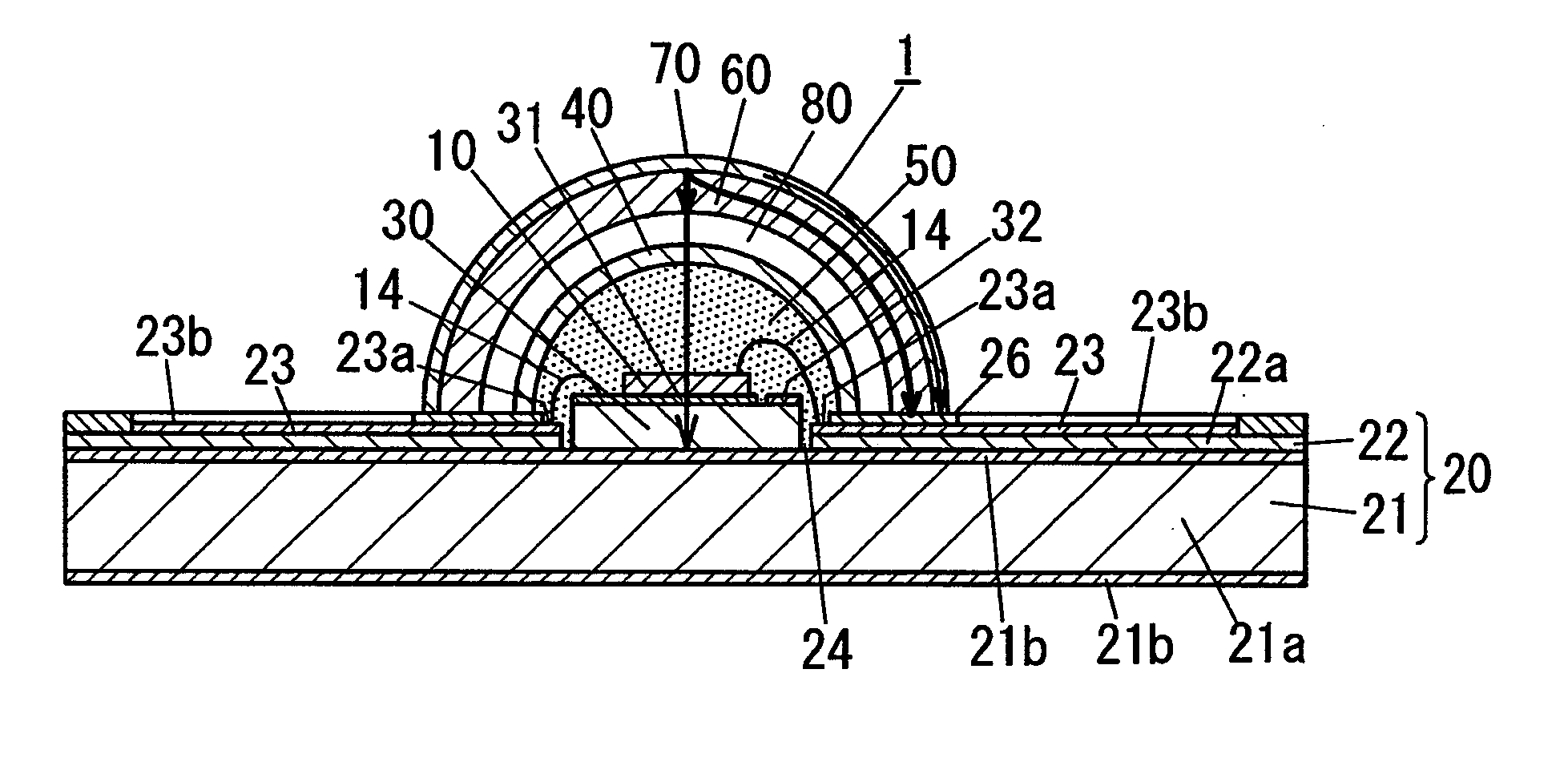
[0043]There is a light emitting device 1 of the present embodiment shown in FIG. 1. The light emitting device 1 includes a LED chip 10 as well as a mounting substrate 20 where the LED chip 10 is mounted. Further, the light emitting device 1 includes a cover member 60 formed to have a dome shape and made of a translucency inorganic material, and a color conversion layer 70 formed to have a dome shape and made of a translucency material including a fluorescent material excited by light emitted from the LED chip 10 and emitting light longer in wavelength than the light emitted from the LED chip 10. The cover member 60 is attached to the mounting substrate 20 such that there is an air layer 80 interposed between the cover member 60 and the mounting substrate 20. The color conversion layer 70 is superposed on a light-outgoing surface of the cover member 60.

[0044]In addition, the light emitting device 1 includes a translucency encapsulation member 50 and an optical member 40. The transluc...

embodiment 2

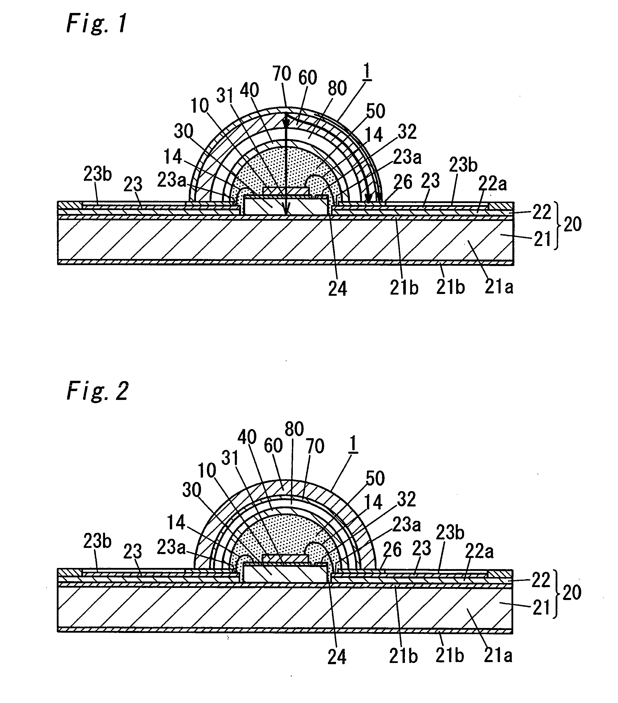
[0067]As shown in FIG. 2, the light emitting device 1 of the present embodiment is different from the light emitting device 1 of the embodiment 1 in that the color conversion layer 70 is superposed on a light-incoming surface, at which the light enters into the cover member 60, of the cover member 60 and the air layer 80 is formed to be interposed between the optical member 40 and the color conversion layer 70. The light emitting device 1 of the present embodiment has a basic structure similar to the embodiment 1. Therefore like parts are designated by like reference numerals and dispensed with duplicate explanations.

[0068]In the light emitting device 1, as described in the above, the color conversion layer 70 is superposed on the light-incoming surface of the cover member 60 and the air layer 80 is formed to be interposed between the optical member 40 and the color conversion layer 70. Therefore, the color conversion layer 70 can be protected with the cover member 60.

[0069]Accordin...

embodiment 3

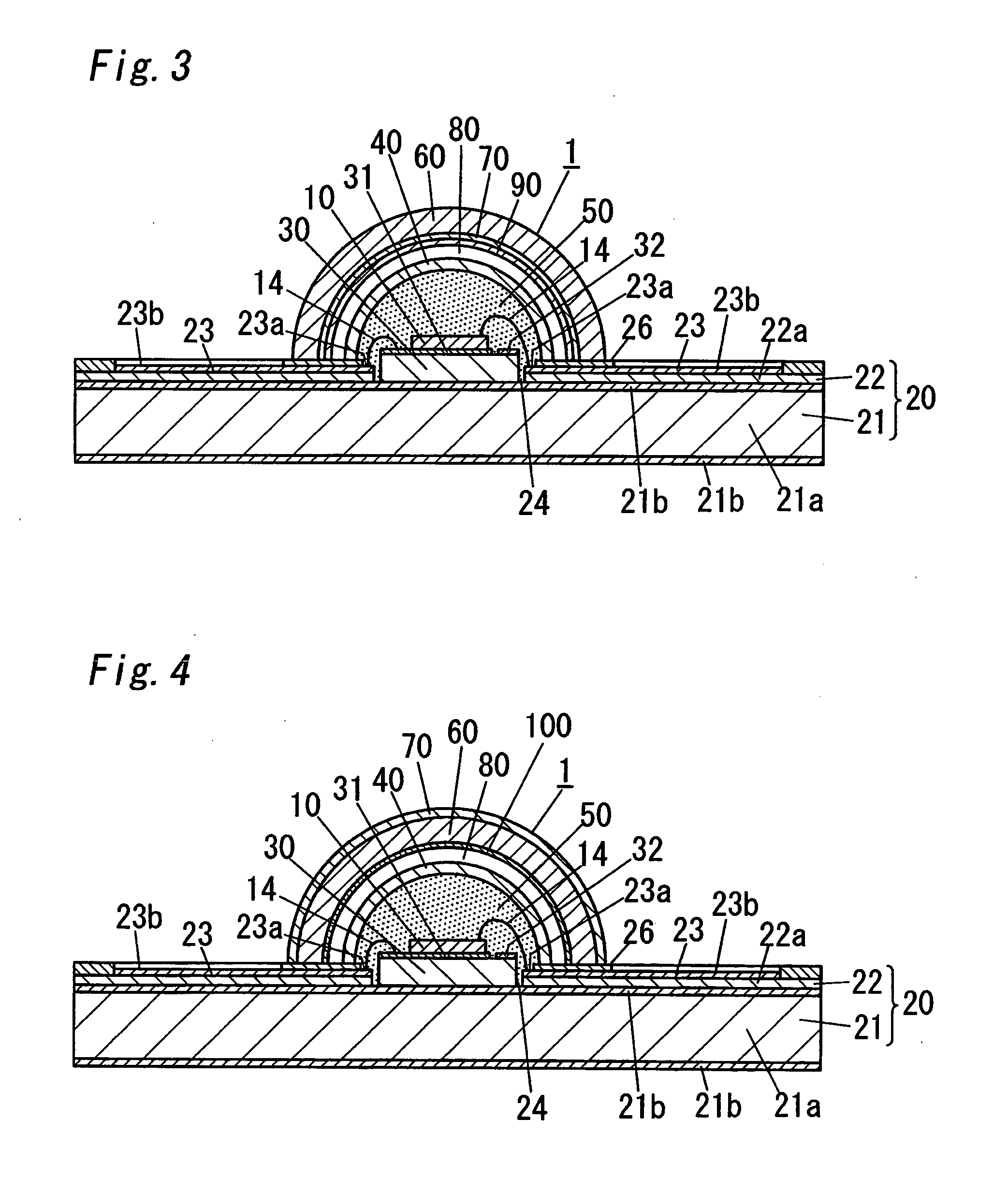
[0070]As shown in FIG. 3, the light emitting device 1 of the present embodiment is different from the light emitting device 1 of the embodiment 2 in that there is a translucency material layer 90 superposed on the color conversion layer 70 superposed on the light-incoming surface of the cover member 60 and the air layer 80 is formed to be interposed between the optical member 40 and the translucency material layer 90. The light emitting device 1 of the present embodiment has a basic structure similar to the embodiment 2. Therefore like parts are designated by like reference numerals and dispensed with duplicate explanations.

[0071]The translucency material layer 90 is, for example, made of a translucency inorganic material (e.g. glass and the like). The translucency material layer 90 is superposed on the color conversion layer 70 so as to cover an entire surface of the color conversion layer 70 opposite to the cover member 60.

[0072]Accordingly, the light emitting device 1 of the pres...


PUM


Abstract

A light emitting device (1) includes a LED chip (10) as well as a mounting substrate (20) on which the LED chip (10) is mounted. Further, the light emitting device (1) includes a cover member (60) and a color conversion layer (70). The cover member (60) is formed to have a dome shape and is made of a translucency inorganic material. The color conversion layer (70) is formed to have a dome shape and is made of a translucency material (such as, a silicone resin) including a fluorescent material excited by light emitted from the LED chip (10) and emitting light longer in wavelength than the light emitted from the LED chip (10). The cover member (60) is attached to the mounting substrate (20) such that there is an air layer (80) between the cover member (60) and the mounting substrate (20). The color conversion layer (70) is superposed on a light-incoming surface or a light-outgoing surface of the cover member (60).

Description

TECHNICAL FIELD[0001]The present invention is directed to a light emitting device utilizing a LED chip (light emitting diode chip).BACKGROUND ART[0002]In the past, there has been proposed a light emitting device utilizing a LED chip. This kind of the light emitting device generally employs a fluorescent material excited by light emitted from the LED chip and emitting light of a color different from a color of the light emitted from the LED chip in order to light having a desired color (for example, white) by means of color mixture of light.[0003]For example, Japanese Patent Publication No. 3978451 discloses a light emitting device 101 shown in FIG. 10. The light emitting device 101 includes a LED chip 110, a mounting substrate 120 on which the LED chip 101 is mounted, a translucency encapsulation member 150, and a color conversion member 170. The translucency encapsulation member 150 is shaped into a semispherical shape and encapsulates the LED chip 110 on a surface of the mounting ...

Claims


Application Information

Patent Timeline
Patent Type & Authority Applications(United States)
IPC IPC(8): H01L33/50H01L33/44H01L33/58H01L33/60H01L33/64
CPCH01L33/507H01L33/58H01L33/60H01L33/644H01L2224/48091H01L2924/00014
Inventor YAMAZAKI, KEIICHITAKEI, NAOKONAKAJIMA, TOMOYUKI
Owner PANASONIC CORP
Why Eureka
Try Eureka