Multilayer wiring substrate, stack structure sensor package, and method of manufacturing stack structure sensor package

a sensor package and wiring substrate technology, applied in the direction of basic electric elements, color television, television systems, etc., can solve the problems of high disposal cost, limited above-mentioned structure, and limited manufacturing location, so as to improve the connection strength of the sensor component and make the structure small and thin.

Active Publication Date: 2010-09-30
SONY CORP
View PDF30 Cites 84 Cited by
  • Summary
  • Abstract
  • Description
  • Claims
  • Application Information

AI Technical Summary

Benefits of technology

[0008]However, the above-mentioned structure is limited to a stack-up manufacturing process in which the integrated circuit 4 is joined after the cavity 3 is formed by the first substrate 1 and the second substrate 2. This has the following disadvantages.
[0013]It is desirable to provide a multilayer wiring substrate, a stack structure sensor package, and a method of manufacturing the stack structure sensor package that enable a sensor component to be reused even when a failure occurs during manufacture, improve connection strength of the sensor component, and make the structure small and thin.
[0017]According to the embodiments of the present invention, it is possible to reuse a sensor component even when a failure occurs during manufacture of a sensor package having a stack structure, to improve connection strength of the sensor component, and to make the structure small and thin.

Problems solved by technology

However, the above-mentioned structure is limited to a stack-up manufacturing process in which the integrated circuit 4 is joined after the cavity 3 is formed by the first substrate 1 and the second substrate 2.
Since the stack-up in the same process step is necessary, a manufacturing location is limited.
Besides, occurrence of a failure causes a high disposal cost.
However, there may be a problem with connection strength because a joint area is limited to the bottom surface.

Method used


Image

  • Multilayer wiring substrate, stack structure sensor package, and method of manufacturing stack structure sensor package
  • Multilayer wiring substrate, stack structure sensor package, and method of manufacturing stack structure sensor package
  • Multilayer wiring substrate, stack structure sensor package, and method of manufacturing stack structure sensor package

Examples


embodiment

1. Embodiment

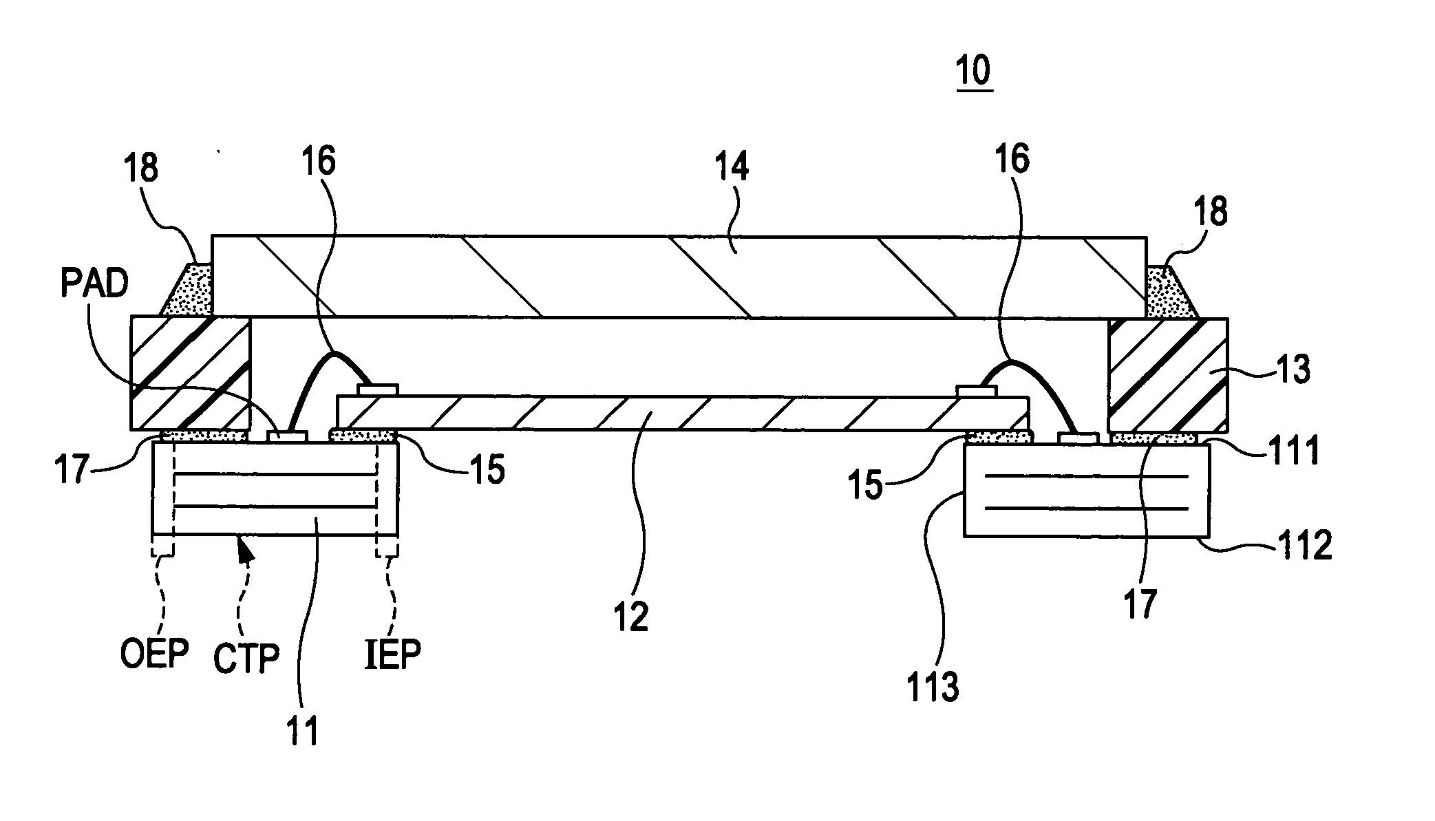
[0032]FIG. 2 illustrates a structure example of a stack structure sensor package to which a multilayer wiring substrate is applied according to an embodiment of the present invention.

[0033]A sensor package 10 has a stack structure that basically includes a multilayer wiring substrate 11, an image sensor chip 12, a frame 13 formed of ceramic, a resin, or the like, and an optical filter 14 as main components.

[0034]The multilayer wiring substrate 11 is a substrate that serves as a base of the stack structure sensor package 10 of an image sensor, and has the following characteristic structure.

[0035]A through hole 113 that passes from a first surface (front surface) 111 through to a second surface (back surface) 112 is formed in a center portion of the multilayer wiring substrate 11.

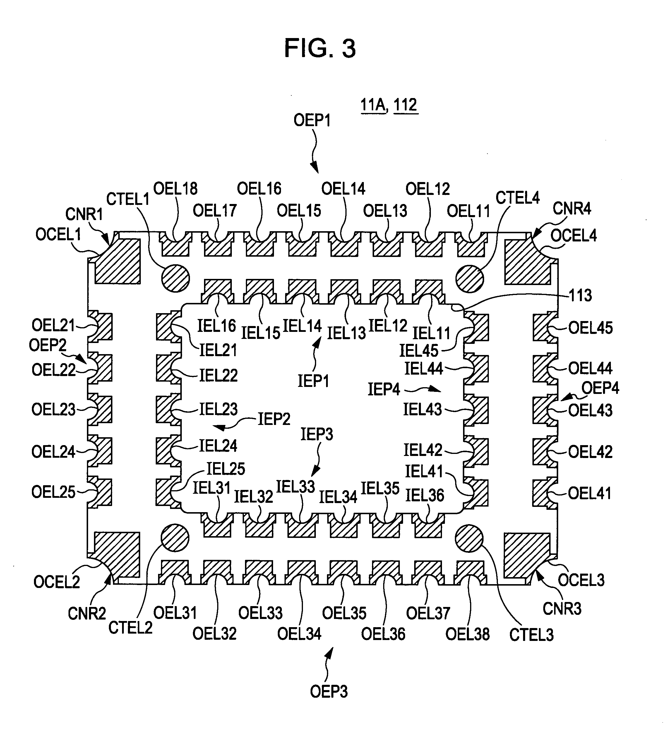
[0036]In the multilayer wiring substrate 11, an electrical connection terminal (electrode) is formed in at least one of an inner edge portion IEP which is a periphery of the through hole 113, an ...


PUM


Abstract

A multilayer wiring substrate has a through hole that passes from a first surface through to a second surface. The multilayer wiring substrate includes an electrical connection terminal formed in at least one of an inner edge portion which is a periphery of the through hole, an outer edge portion which is an outer periphery of the substrate, and a non-edge portion, on at least one of the first surface and the second surface. The electrical connection terminal has a castellation structure that does not pass through to a surface opposite to a formation surface.

Description

BACKGROUND OF THE INVENTION[0001]1. Field of the Invention[0002]The present invention relates to a multilayer wiring substrate, a stack structure sensor package, and a method of manufacturing the stack structure sensor package that are applied to an image sensor and the like.[0003]2. Description of the Related Art[0004]Japanese Unexamined Patent Application Publication No. 2002-353427 proposes a stack structure sensor package of an image sensor.[0005]FIG. 1 illustrates the stack structure sensor package of the image sensor as disclosed in Japanese Unexamined Patent Application Publication No. 2002-353427.[0006]In a sensor package structure in FIG. 1, a frame-shaped second substrate 2 is joined onto a first surface of a first substrate 1, thereby forming a cavity 3.[0007]An integrated circuit 4 is mounted on the first surface of the first substrate 1 in the cavity 3, and an image sensor chip 5 is joined onto the second substrate 2. Thus, the stack structure sensor package is formed.S...

Claims


Application Information

Patent Timeline
Patent Type & Authority Applications(United States)
IPC IPC(8): H01L31/0232H05K1/11H01L31/18H01L23/12H01L27/14H01L31/02H04N5/335
CPCH01L24/16H01L24/31H01L2924/19105H01L2924/19043H01L2924/16195H01L2924/15311H01L2924/15156H01L2924/14H01L2924/01079H01L2924/01078H01L2224/73265H01L2224/48227H01L2224/48091H01L2224/32225H01L2224/32014H01L24/48H01L27/14618H01L27/14621H01L27/14683H01L31/0203H01L2224/16H01L2924/00014H01L2924/00H01L2924/00012H01L2924/15151H01L24/73H01L2224/04042H01L2224/92247H01L2924/00011H01L2924/15157H01L2224/0401H01L2224/45099H01L2224/45015H01L2924/207H01L2224/32245H01L2224/48247
Inventor SHIBUTA, NORIKOTERASAKI, TOHRUYAMADA, TOMOYASUNAITO, NOBUOTSUKUDA, YUKIHIKONONOYAMA, RYU
Owner SONY CORP
Why Eureka
Try Eureka