LED package with increased feature sizes

Active Publication Date: 2010-10-07
CREELED INC
View PDF99 Cites 140 Cited by
  • Summary
  • Abstract
  • Description
  • Claims
  • Application Information

AI Technical Summary

Benefits of technology

[0013]A light emitter package according to an embodiment of the present invention comprises the following elements. A light emitter chip is disposed

Problems solved by technology

While a package such as the package 20 illustrated in FIG. 1B may have certain advantages for high power operation, there may be a number of potential problems associated with using a separate metal piece as a metal reflector.
For example, small metal parts may be difficult to manufacture repeatable with a hig

Method used


Image

  • LED package with increased feature sizes
  • LED package with increased feature sizes
  • LED package with increased feature sizes

Examples


Embodiment Construction

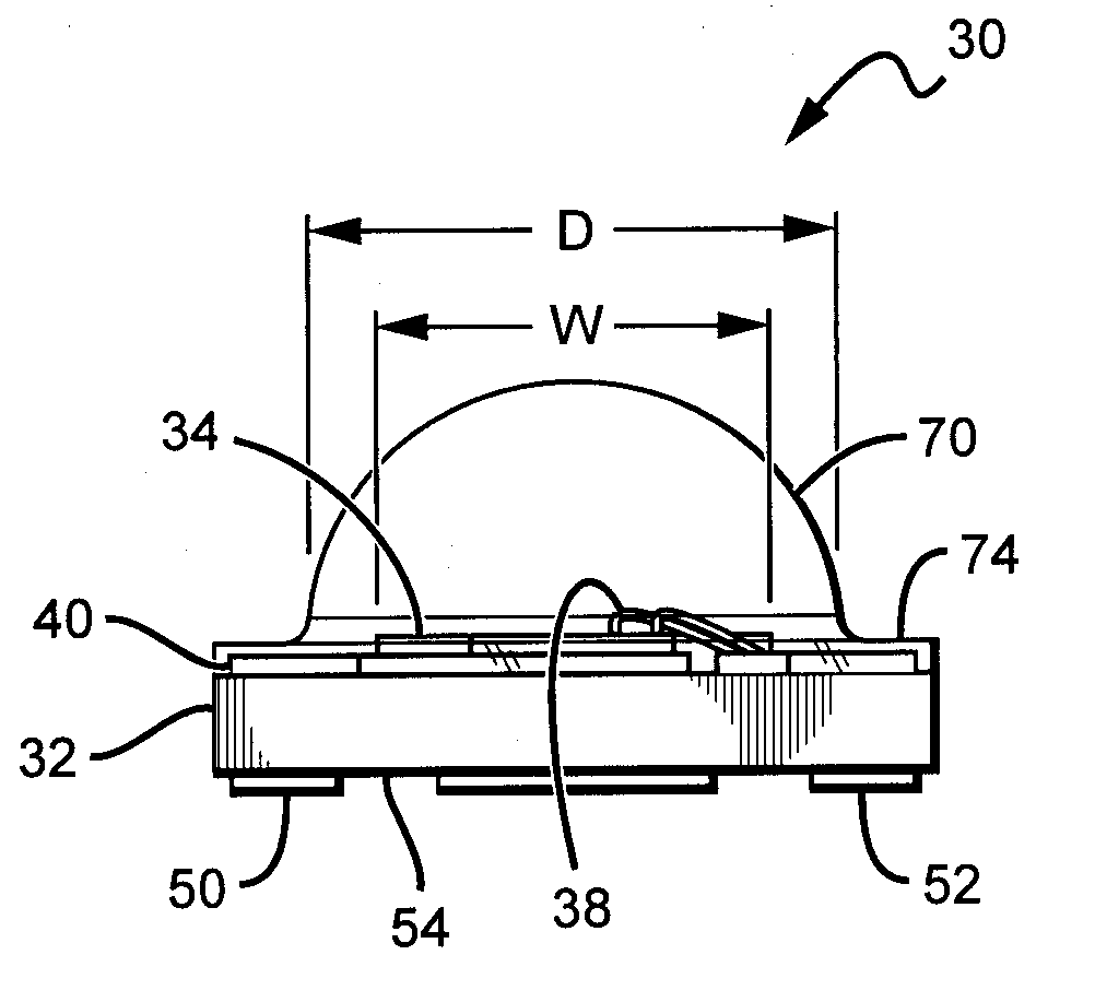
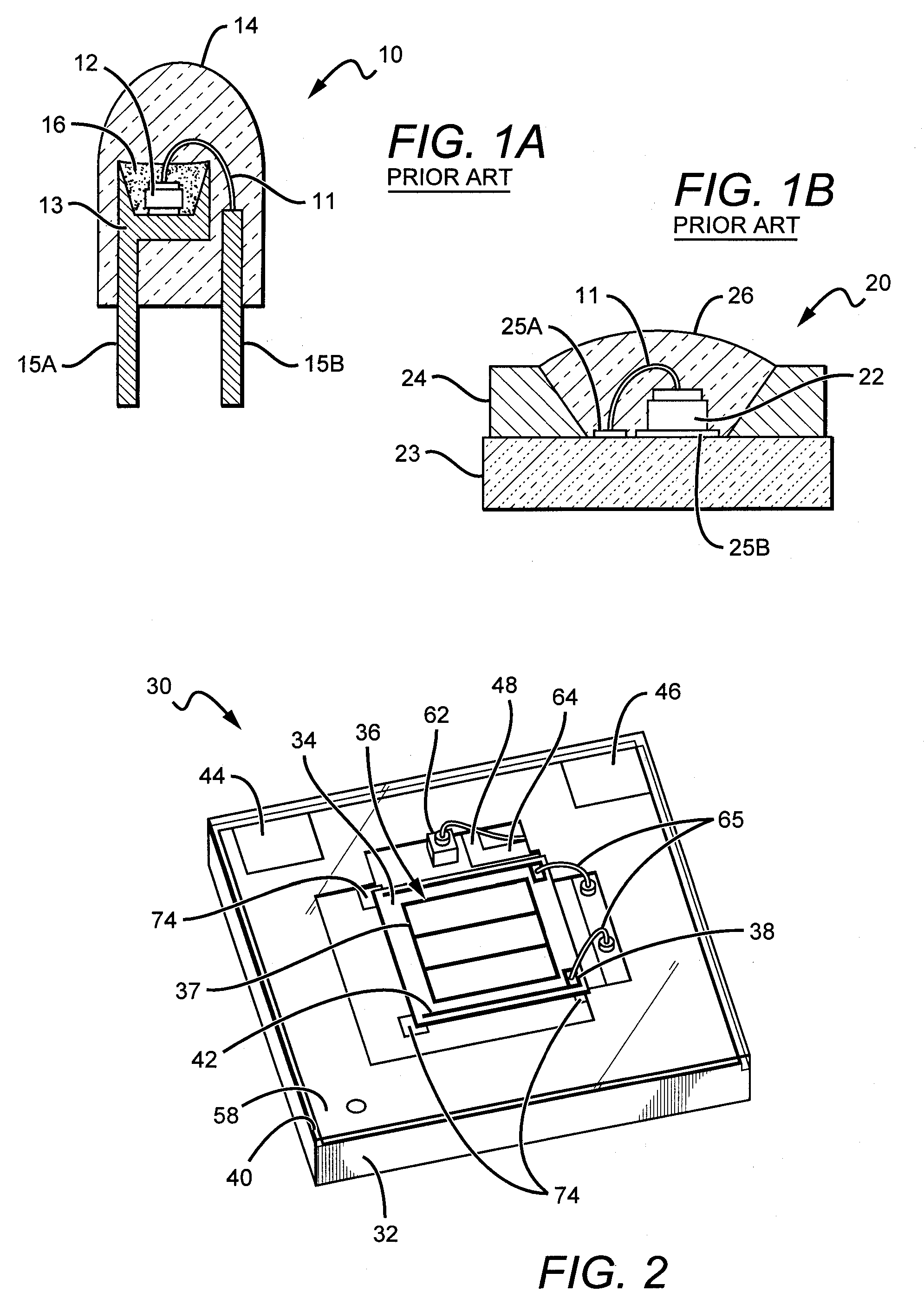
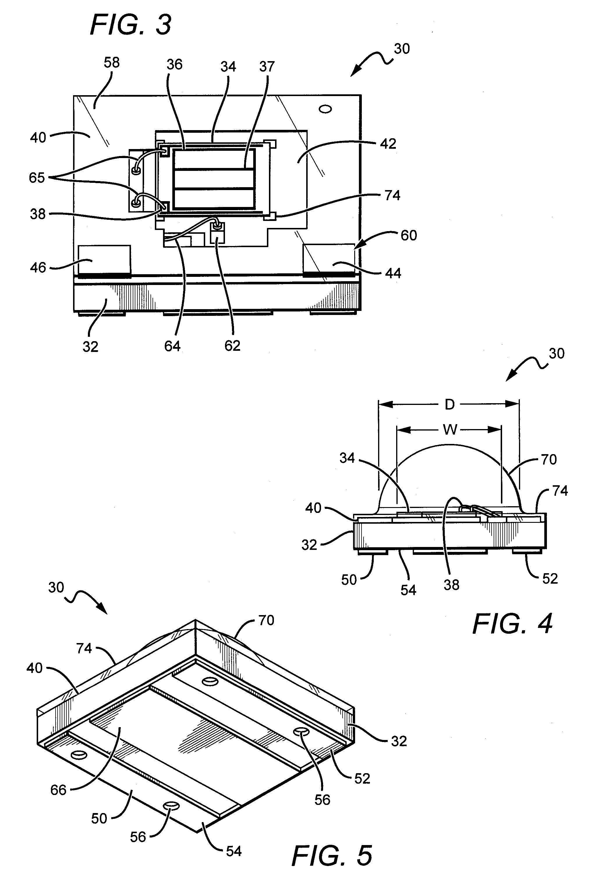
[0028]The present invention is directed to compact, simple and efficient high power LED packages and methods for manufacturing same. Different embodiments can comprise one or more high power LEDs that typically operate at elevated power levels and temperatures. Packages according to the present invention can include features that allow for higher output power with still provided for thermal management by arranging features to help spread the heat from the LED. The heat can then dissipate into the ambient. The packages according to the present invention can also comprise a lens molded directly over the one or more LEDs to protect the LED while still allowing for efficient emission characteristics.

[0029]In conventional LED packages, light is most efficiently extracted through the molded lens for LEDs when the ratio of the width of the LED chip to the lens diameter is relatively low. LED chips with a smaller footprint (or width) compared to the diameter of the lens more closely emulate...


PUM


Abstract

A light emitter package having increased feature sizes for improved luminous flux and efficacy. An emitter chip is disposed on a submount with a lens that covers the emitter chip. In some cases, the ratio of the width of the light emitter chip to the width of said lens in a given direction is 0.5 or greater. Increased feature sizes allow the package to emit light more efficiently. Some packages include submounts having dimensions greater than 3.5 mm square used in conjunction with larger emitter chips. Materials having higher thermal conductivities are used to fabricate the submounts, providing the package with better thermal management.

Description

[0001]This application is a continuation-in-part of prior U.S. patent application Ser. No. 11 / 982,275, filed 31 Oct. 2007. This application claims the benefit of U.S. Provisional Application No. 61 / 173,550, filed 28 Apr. 2009.BACKGROUND OF THE INVENTION[0002]1. Field of the Invention[0003]This invention relates to light emitter packages, and in particular to light emitting diode (LED) packages having a molded lens.[0004]2. Description of the Related Art[0005]Light emitting diodes (LED or LEDs) are solid state devices that convert electric energy to light, and generally comprise one or more active layers of semiconductor material sandwiched between oppositely doped layers. When a bias is applied across the doped layers, holes and electrons are injected into the active layer where they recombine to generate light. Light is emitted from the active layer and from all surfaces of the LED.[0006]In order to use an LED chip in a circuit or other like arrangements, it is known to enclose an ...

Claims


Application Information

Patent Timeline
IPC IPC(8): H01L33/58
CPCH01L33/20H01L33/486H01L33/54H01L33/58H01L33/62H01L2924/01087H01L2224/48091H01L33/641H01L2924/01019H01L2924/00014
Inventor EMERSON, DAVIDCOLLINS, BRIANBERGMANN, MICHAELEDMOND, JOHNTARSA, ERICANDREWS, PETERKELLER, BERNDHUSSELL, CHRISTOPHERSALTER, AMBER
Owner CREELED INC
Why Eureka
Try Eureka