Liquid crystal display device

a liquid crystal display and display panel technology, applied in the field of liquid crystal display panels, can solve the problems of easy deterioration of the properties, and achieve the effects of reducing the number of light emitting diodes, reducing the heat on the above described semiconductor devices, and reducing the heat on the semiconductor devices on the liquid crystal display panel

Inactive Publication Date: 2010-10-07
PANASONIC LIQUID CRYSTAL DISPLAY CO LTD +1
View PDF3 Cites 4 Cited by
  • Summary
  • Abstract
  • Description
  • Claims
  • Application Information

AI Technical Summary

Benefits of technology

[0009]In this case, the side of the liquid crystal display panel along which the above described semiconductor device is mounted is located on the same side of the backlight as the side along which a number of light emitting diodes (LED's) are aligned as described above, and as a result, several light emitting diodes are in the proximity of the above described semiconductor device. Therefore, the above described semiconductor device is easily affected by the heat from the light emitting diodes provided in the proximity thereof, and thus, the properties easily deteriorate.
[0011]In FIG. 3, a number of light emitting diodes LD (LD1 in the figure) are provided and aligned along the first side wall WF1 on the side of the light guiding plate GLB where semiconductor devices SEC are provided. These light emitting diodes LD are provided at equal intervals (with a pitch W0 of 14.1 mm for 10.5 inch liquid crystal panels). In this case, there are three semiconductor devices SEC, for example, the width W1 is 19.0 mm, and the distance D between adjacent semiconductor devices SEC is 23.2 mm. Three light emitting diodes DL1 are provided in the proximity of one semiconductor device SEC, and the above described semiconductor devices SEC are easily affected by the heat from the three light emitting diodes DL1.
[0013]In order to avoid the above described disadvantage of the backlight BL having such a structure, it is possible to reduce the number of light emitting diodes LD1 provided in the proximity of the semiconductor devices SEC, as described above, so that the effects of heat on the above described semiconductor devices SEC can be reduced. By doing so, however, it becomes difficult to make the brightness of the backlight BL uniform.
[0014]An object of the present invention is to provide a liquid crystal display device where the effects of heat on the semiconductor devices on the liquid crystal display panel can be reduced and the brightness of the backlight can be made uniform.
[0015]In the liquid crystal display device according to the present invention, a number of light emitting diodes (first light source group) are aligned along the side wall of the side (first side) of the light guiding plate corresponding to the side of the liquid crystal display panel along which semiconductor devices are mounted, and at the same time, a number of light emitting diodes (second light source group) are aligned along the side wall of the side (second side) that faces the above described first side, so that there is a difference in pitch between the light emitting diodes in the above described first light source group, so that the pitch is longer in places where the above described semiconductor devices are located, while there is a difference in pitch between the light emitting diodes in the above described second light source group, so that the pitch is shorter in places that correspond to places where the pitch between the light emitting diodes in the above described first light source group is longer.

Problems solved by technology

Therefore, the above described semiconductor device is easily affected by the heat from the light emitting diodes provided in the proximity thereof, and thus, the properties easily deteriorate.

Method used


Image

  • Liquid crystal display device
  • Liquid crystal display device
  • Liquid crystal display device

Examples


first embodiment

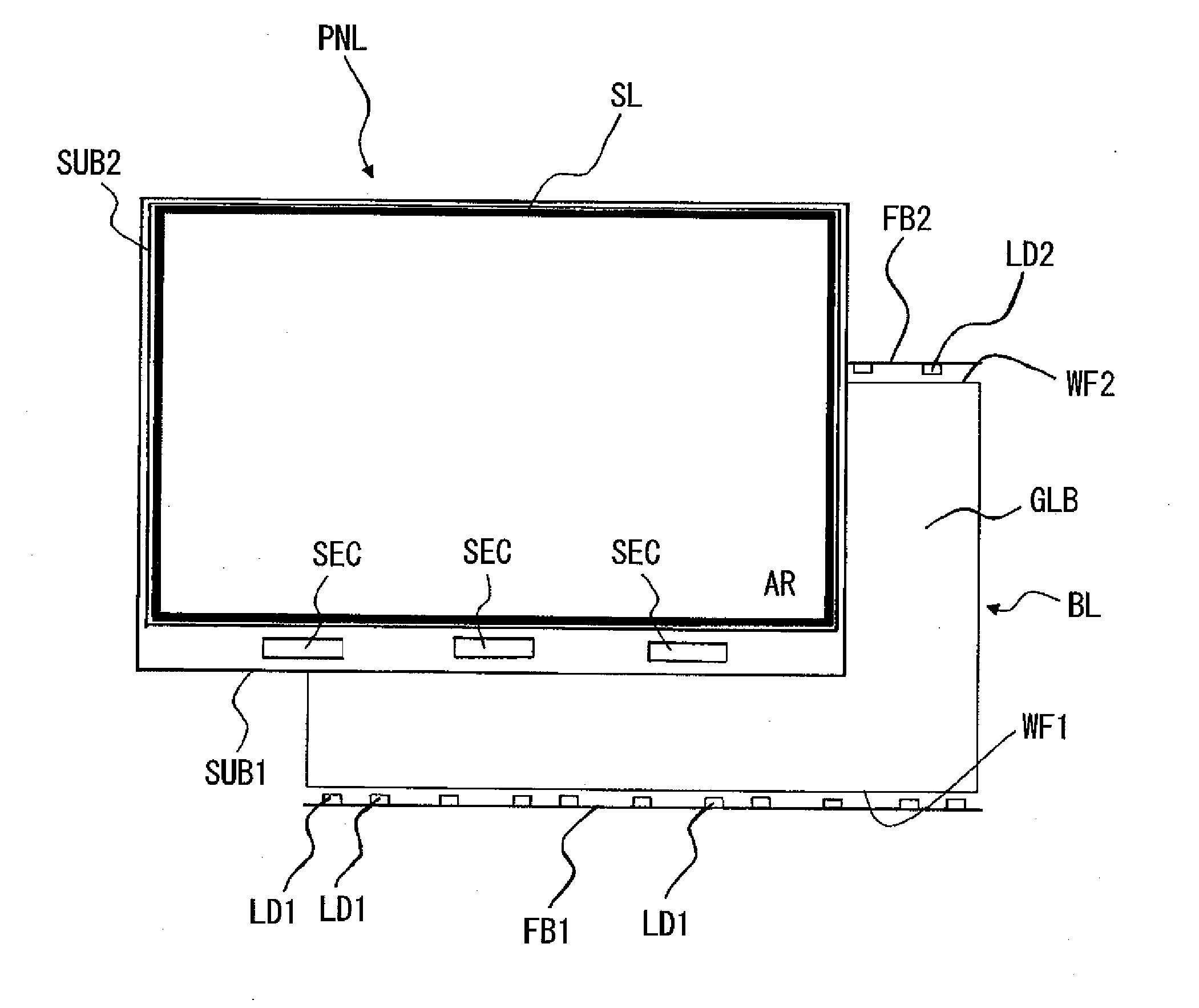
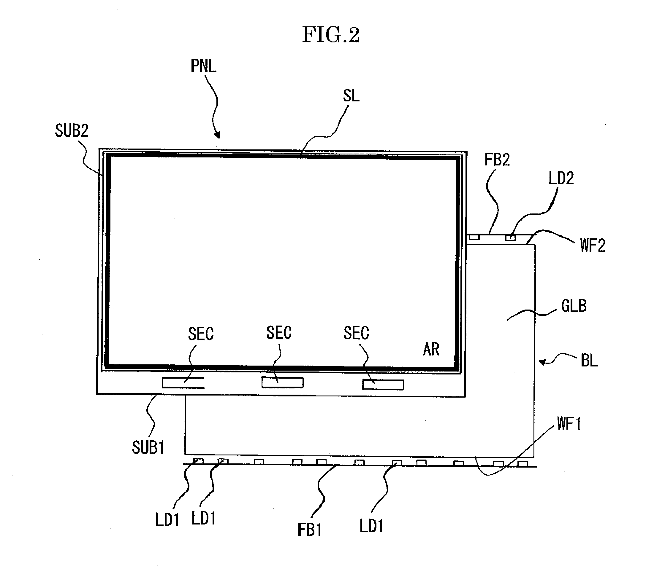
[0044]FIG. 2 is a plan diagram showing the liquid crystal display device according to the first embodiment of the present invention. The liquid crystal display device is formed of a liquid crystal display panel PNL and a backlight BL provided in the rear of the liquid crystal display panel PNL. Though in FIG. 2 the backlight BL is not aligned with the liquid crystal display panel PNL, the backlight BL is actually provided so as to perfectly overlap with the rear of the liquid crystal display panel PNL.

[0045]The liquid crystal display panel PNL is formed of a housing made of a substrate SUB1 and a substrate SUB2 which are positioned so as to face each other and sandwich liquid crystal (not shown). The substrate SUB2 is provided so as to overlap with the above described substrate SUB1 in such a manner that the lower side of the substrate SUB1 in the figure is slightly exposed, for example, and secured to the above described substrate SUB1 with an annular sealing material SL formed aro...

second embodiment

[0060]FIG. 4A is a diagram showing the liquid crystal display device according to another embodiment of the present invention, and corresponds to FIG. 1. FIG. 4B is a cross sectional diagram along line b-b in FIG. 4A.

[0061]In FIG. 4A, the state of alignment of the light emitting diodes LD1 and the state of alignment of the light emitting diodes LD2 is the same as in FIG. 1.

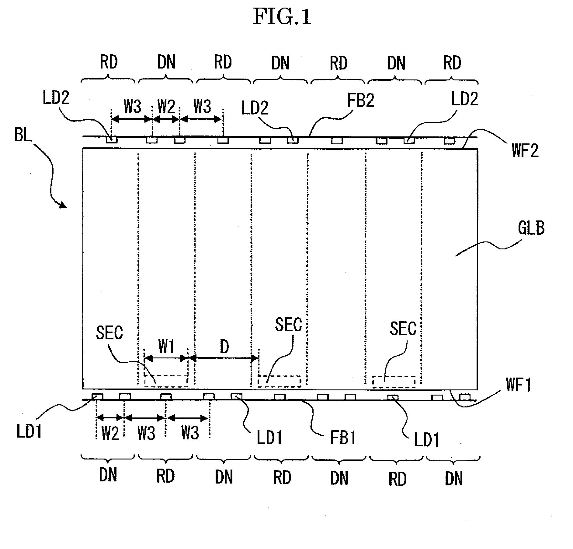
[0062]What is different from the case in FIG. 1 is that recesses DNT are provided (DNT1 in the figure) in portions corresponding to regions (RD) where light emitting diodes LD1 are scarce both on the front and rear surface of the light guiding plate GLD on the side wall WF1 side. These recesses DNT1 extend to the middle of the light guiding plate GLB in a direction perpendicular to the direction in which light emitting diodes LD1 are aligned, and are created so as to become shallower in the direction in which they extend, for example. Likewise, recesses DNT (DNT2 in the figure) are created in portions correspondin...


PUM

PropertyMeasurementUnit
distanceaaaaaaaaaa
width W1aaaaaaaaaa
width W1aaaaaaaaaa

Abstract

The present invention provides a liquid crystal display device, wherein the backlight has a light guiding plate, a first light source group made up of light sources aligned along a first side of the light guiding plate and a second light source group made up of light sources aligned along a second side that faces the first side, the first light source group has a first region where the distance between adjacent light sources is a first distance and a second region where the distance between adjacent light sources is a second distance that is smaller than the first distance, the second light source group has a third region facing the first region and a fourth region facing the second region, the third distance between adjacent light sources in the third region is smaller than the fourth distance between adjacent light sources in the fourth region, and semiconductor devices are positioned so as to face the first region.

Description

CROSS-REFERENCE TO RELATED APPLICATION[0001]The present application claims priority over Japanese Application JP2009-092864 filed on Apr. 7, 2009, the contents of which are hereby incorporated into this application by reference.BACKGROUND OF THE INVENTION[0002](1) Field of the Invention[0003]The present invention relates to a liquid crystal display device, and in particular, to a liquid crystal display device having a liquid crystal display panel and a backlight of a so-called edge light type provided on the rear of this liquid crystal display panel.[0004](2) Description of the Related Art[0005]Liquid crystal display panels have such a structure that the amount of light that transmits through the pixels that form the image display region of the panel can be controlled, and therefore, the backlight of liquid crystal display panels is usually provided in the rear.[0006]There are backlights of an edge light type, for example, which are formed of a light guiding plate that is positioned...

Claims


Application Information

Patent Timeline
Patent Type & Authority Applications(United States)
IPC IPC(8): G02F1/13357
CPCG02F1/133615G02B6/002G02B6/0045G02B6/0068G02B6/0073G02B6/0085
Inventor TOMIZUKA, YOSHITERU
Owner PANASONIC LIQUID CRYSTAL DISPLAY CO LTD
Why Eureka
Try Eureka