Display

Active Publication Date: 2008-09-02
SANYO ELECTRIC CO LTD
View PDF4 Cites 12 Cited by
  • Summary
  • Abstract
  • Description
  • Claims
  • Application Information

AI Technical Summary

Benefits of technology

[0010]The present invention has been proposed in order to provide

Problems solved by technology

In the conventional bootstrap inverter circuit shown in FIG. 19, however, the potential of the node ND101 is in excess of VDD as described above, and hence a bias voltage applied to the transistor NT104 connected to VSS disadvantageously exceeds the potential difference between VDD and VSS.
Therefore, the properties of the transistor NT104 tend disadvan

Method used


Image

  • Display
  • Display
  • Display

Examples


first embodiment

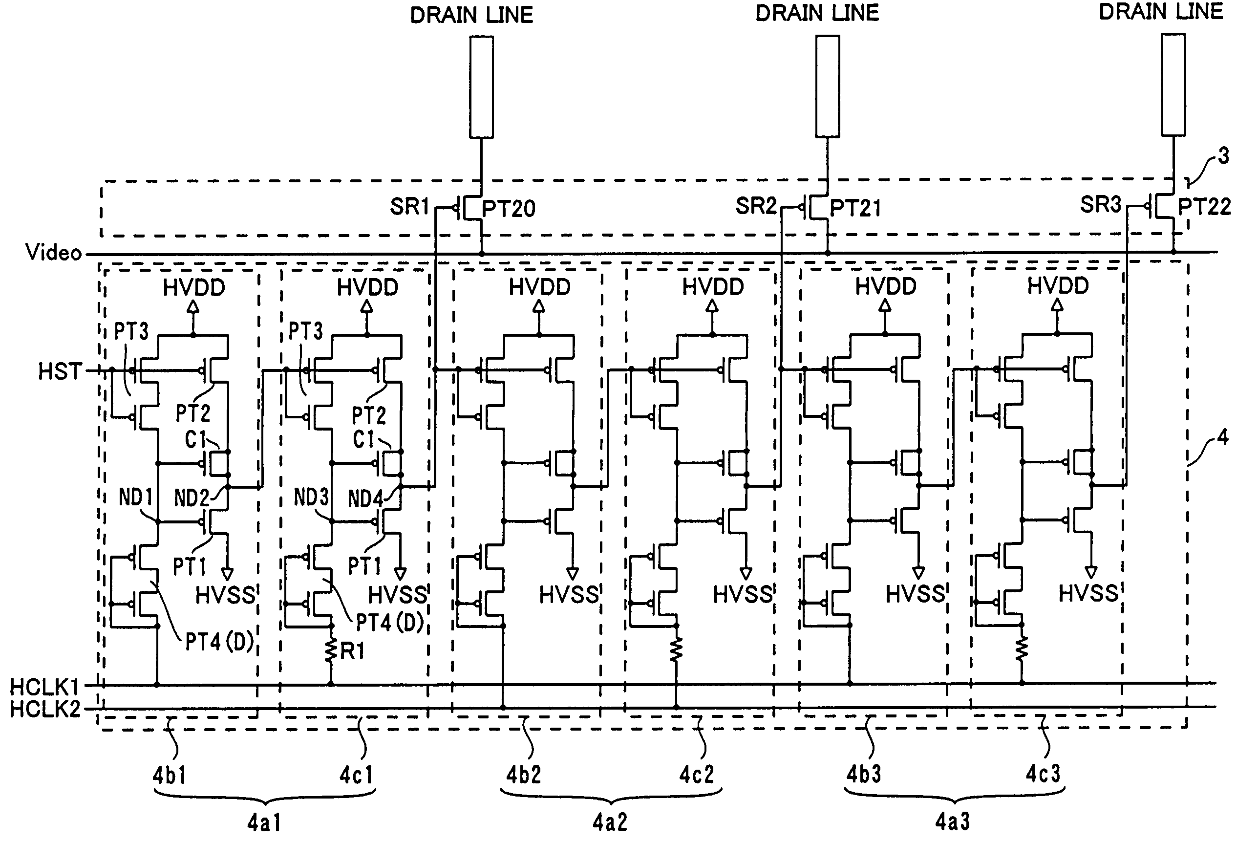
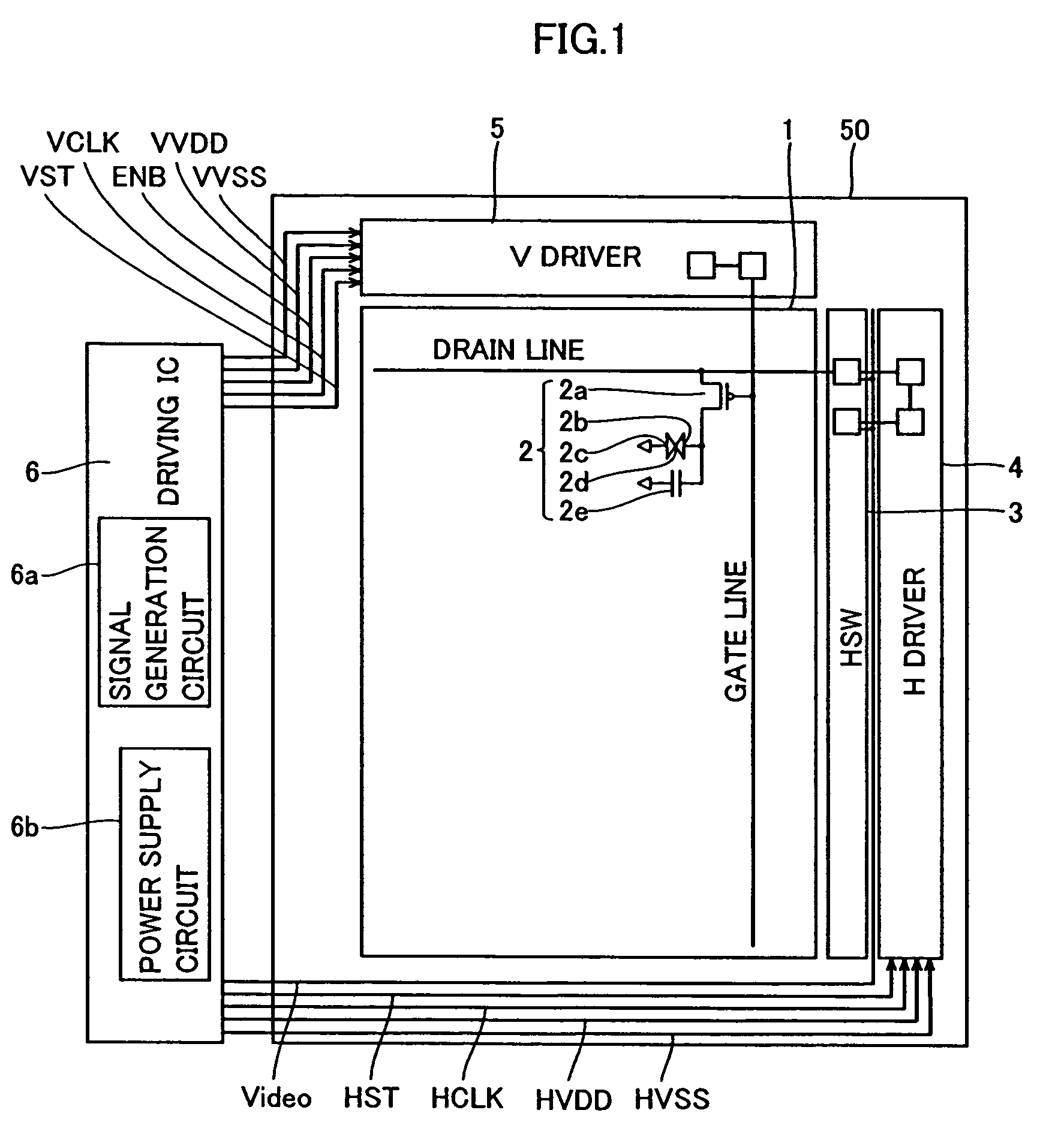
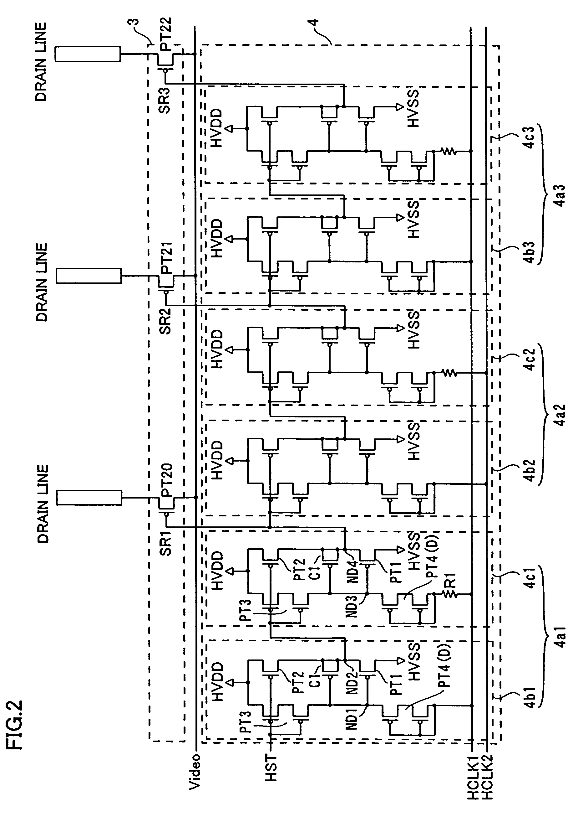
[0034]Referring to FIG. 1, a display part 1 is provided on a substrate 50 in a liquid crystal display according to a first embodiment of the present invention. The display part 1 is illustrated in a structure for one pixel 2 in FIG. 1. Such pixels 2 are arranged on the display part 1 in the form of a matrix. Each pixel 2 is constituted of a p-channel transistor 2a, a pixel electrode 2b, an opposing electrode (common electrode) 2c, common to the respective pixels 2, arranged oppositely to the pixel electrode 2b, a liquid crystal 2d held between the pixel electrode 2b and the common electrode 2c and a storage capacitor 2e. The p-channel transistor 2a has a source connected to a drain line, a drain connected to the pixel electrode 2b and the storage capacitor 2e, and a gate connected to a gate line.

[0035]A horizontal switch (HSW) 3 and an H driver 4 are provided on the substrate 50 along one side of the display part 1, in order to drive (scan) drain lines thereof. A V driver 5 is provi...

second embodiment

[0065]Referring to FIG. 5, the present invention is applied to a V driver 5 for driving (scanning) gate lines in a liquid crystal display according to a second embodiment of the present invention, dissimilarly to the aforementioned first embodiment.

[0066]As shown in FIG. 5, the V driver 5 of the liquid crystal display according to the second embodiment is provided with a plurality of stages of shift register circuits 5a1 and 5a2. FIG. 5 shows only two shift register circuits 5a1 and 5a2, for simplifying the illustration. The first-stage shift register circuit 5a1 is constituted of 1st, 2nd and 3rd first circuit parts 5b11, 5b12 and 5b13 and a second circuit part 5c1. The 1st first circuit part 5b11 includes transistors PT1, PT2 and PT3, a diode-connected transistor PT4 and a capacitor C1 formed by connecting the source and the drain of a transistor with each other. The 2nd circuit part 5c1 includes transistors PT11, PT12, PT13 and PT14 and a capacitor C11 corresponding to the transi...

third embodiment

[0096]In a liquid crystal display according to a third embodiment of the present invention, an H driver for driving (scanning) drain lines is constituted of n-channel transistors.

[0097]Referring to FIG. 7, a display part 11 is provided on a substrate 60 in the liquid crystal display according to the third embodiment. FIG. 7 shows the display part 11 in a structure for one pixel 12. Each of the pixels 12 arranged on the display part 11 in the form of a matrix is constituted of an n-channel transistor 12a, a pixel electrode 12b, an opposing electrode (common electrode) 12c, common to the respective pixels 12, arranged oppositely to the pixel electrode 12b, a liquid crystal 12d held between the pixel electrode 12b and the common electrode 12c and a storage capacitor 12e. The n-channel transistor 12a has a source connected to the pixel electrode 12b and the storage capacitor 12e, a drain connected to a drain line and a gate connected to a gate line. A horizontal switch (HSW) 13 and an H...


PUM


Abstract

A display capable of suppressing reduction of a scanning property is provided. This display comprises a shift register circuit formed by connecting a plurality of first circuit parts each including a first conductivity type first transistor connected to a first potential and turned on in response to a clock signal, a first conductivity type second transistor connected to a second potential and a first conductivity type third transistor, connected between the gate of the first transistor and the second potential, having two gate electrodes electrically connected with each other.

Description

BACKGROUND OF THE INVENTIONField of the Invention[0001]The present invention relates to a display, and more particularly, it relates to a display having a shift register circuit.CROSS-REFERENCE TO RELATED APPLICATIONS[0002]The priority application number JP2003-185263 upon which this patent application is based is hereby incorporated by reference.Description of the Background Art[0003]A bootstrap inverter circuit is known in general, as disclosed in Japanese Patent No. 2921510 (IPC: H03K 19 / 094), for example.[0004]FIG. 19 is a circuit diagram showing a conventional bootstrap inverter circuit. Referring to FIG. 19, the conventional bootstrap inverter circuit includes n-channel transistors NT101, NT102, NT103 and NT104 and a capacitor C101. The transistor NT101 has a source connected to a node ND102, a drain connected to a positive potential VDD and a gate connected to another node ND101. The capacitor C101 is connected between the gate and the source of the transistor NT101. The tran...

Claims


Application Information

Patent Timeline
IPC IPC(8): G09G3/36G02F1/133G09G3/20G09G3/30G09G3/32G11C19/00G11C19/18G11C19/28H01L51/50H03K19/0175
CPCG11C19/28G11C19/00G11C19/184G09G3/3266G09G3/3275G09G3/3677G09G3/3688G09G2310/0275G09G2310/0267G09G3/36G09G3/20
Inventor SENDA, MICHIRU
Owner SANYO ELECTRIC CO LTD
Why Eureka
Try Eureka