Fingerprint sensor chip package method and the package structure thereof

a fingerprint sensor and chip technology, applied in the field of semiconductor chip package methods and the package structure thereof, to achieve the effects of dissipating static charges, improving product yields, and reducing package thickness

Active Publication Date: 2010-10-14
APTOS TECH
View PDF1 Cites 17 Cited by
  • Summary
  • Abstract
  • Description
  • Claims
  • Application Information

AI Technical Summary

Benefits of technology

[0007]In order to solve aforementioned problems, an objective of the present invention is to provide a package method of a fingerprint sensor chip and the package structure thereof which replaces metal bond wires of the prior art with a conductive co

Problems solved by technology

However, some newly developed chip applications requi

Method used


Image

  • Fingerprint sensor chip package method and the package structure thereof
  • Fingerprint sensor chip package method and the package structure thereof
  • Fingerprint sensor chip package method and the package structure thereof

Examples


Embodiment Construction

[0014]The present invention is described with the embodiments below. However, it should be understood that the embodiments are only to exemplify the present invention but not to limit the scope of the present invention.

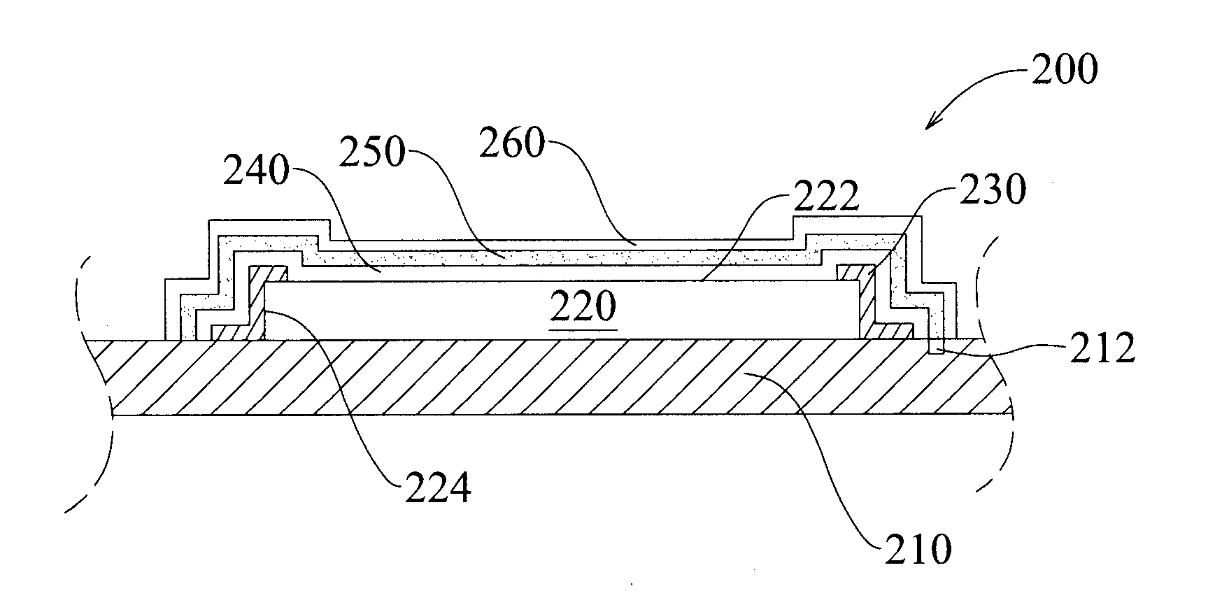
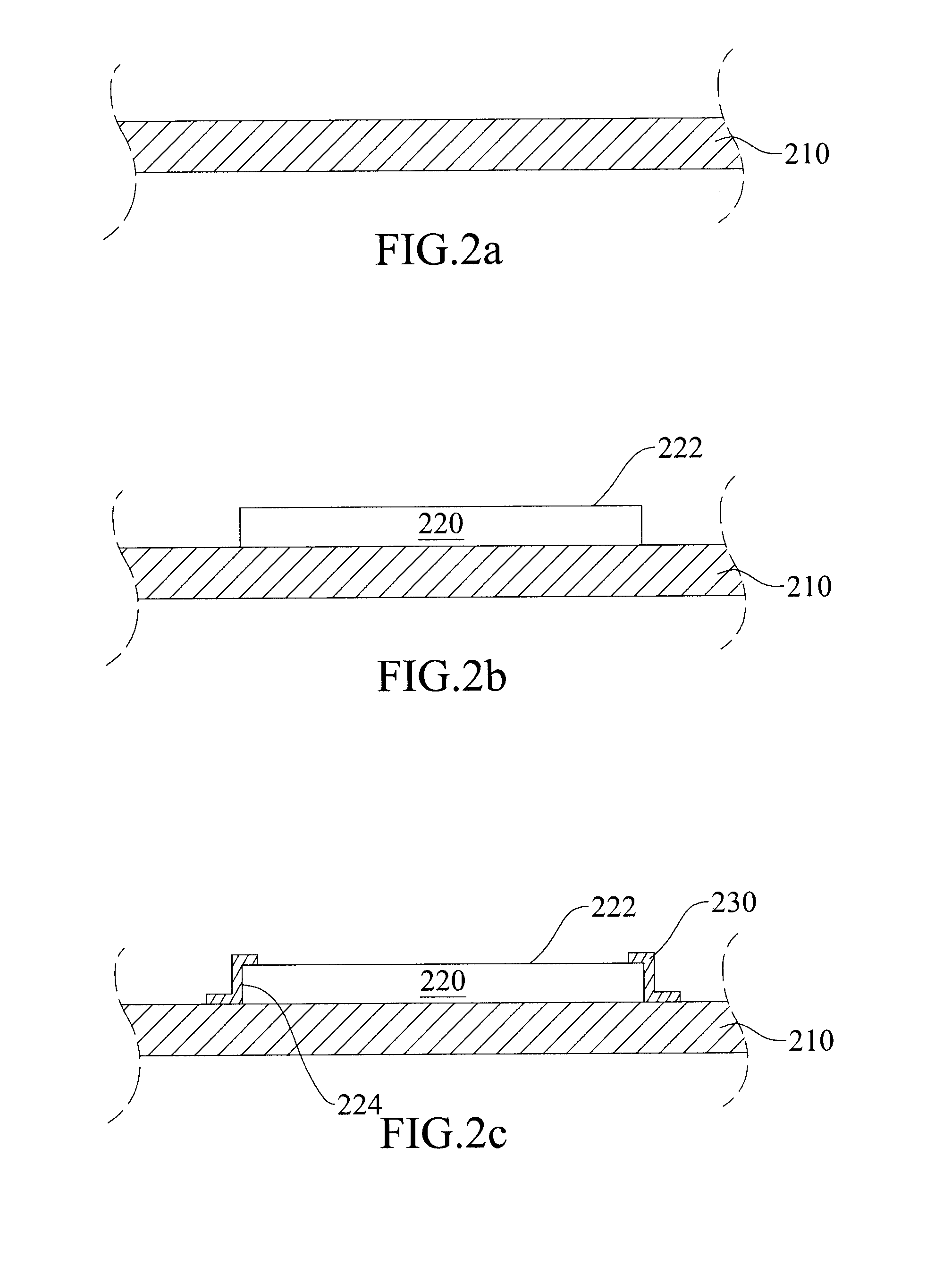
[0015]Please referring to FIG. 2a to FIG. 2e, they present the cross-sectional views of the structure at each step of the fingerprint sensor chip package method of the present invention. The fingerprint sensor chip package method includes the following steps. First, referring to FIG. 2a, a substrate 210 having a circuit layer (not shown in the figure) thereon is provided. Referring to FIG. 2b, a sensor chip 220 is arranged on the substrate 210, wherein the active surface 222 of the sensor chip 220 faces upward. In one embodiment, the sensor chip 220 can be affixed to the substrate 210 by adhesives. Next, referring to FIG. 2c, a patterned conductive colloid 230 is formed on the sensor chip 220, wherein the conductive colloid layer 230 extends downwardly from the periph...


PUM


Abstract

A fingerprint sensor chip package method and the package structure thereof are disclosed. The invention includes: providing a substrate; arranging a sensor chip on the substrate, with an active surface of the sensor chip facing upward; forming a patterned conductive colloid on the sensor chip, wherein the patterned conductive colloid extends from the periphery of the active surface of the sensor chip along the side wall of the sensor and electrically connects with the circuit layer of the substrate; forming a non-conductive film to cover the sensor chip, the patterned conductive colloid and a portion of the substrate; and forming a conductive film on the non-conductive film. The patterned conductive colloid replaces the conventional bond wires to improve the product yield and to omit the molding process. The conductive film is electrically connected with the grounding point/area on the substrate to dissipate the static charges for protecting the chip.

Description

BACKGROUND OF THE INVENTION[0001]1. Field of the Invention[0002]The present invention relates to a semiconductor chip package method and the package structure thereof, and more particularly, to a fingerprint sensor chip package method and the package structure thereof.[0003]2. Description of the Prior Art[0004]Chip fabrication methods provided in the semiconductor fabrication field often need to take the electrical property of a chip into consideration and arrange the chip in a package through package procedures to avoid any possible destruction by external forces such as pressure and electrostatics.[0005]However, some newly developed chip applications require the chip surface to be exposed to the environment. For example, a finger print sensor needs to provide a chip surface to be touched by a finger when reading the pattern of a finger for identification.[0006]FIG. 1 shows the package structure of a touch sensing fingerprint recognition device 100 of a prior art. It mainly include...

Claims


Application Information

Patent Timeline
IPC IPC(8): H01L31/0216H01L21/50
CPCG06K9/00006H01L24/63H01L2224/48091H01L2224/48227H01L2924/01079H01L2924/09701H01L2924/1815H01L2224/45144H01L2924/01047H01L2924/00014H01L2924/00G06V40/12
Inventor JOW, EN-MIN
Owner APTOS TECH
Why Eureka
Try Eureka