Liquid crystal display device and manufacturing method for same
a technology of liquid crystal display and manufacturing method, which is applied in the direction of optics, instruments, electrical equipment, etc., can solve the problems of difficult to reduce the film thickness for flattening, difficult to make half of the film thickness remain, and uneven thickness of the liquid crystal layer
- Summary
- Abstract
- Description
- Claims
- Application Information
AI Technical Summary
Benefits of technology
Problems solved by technology
Method used
Image

Examples
first embodiment
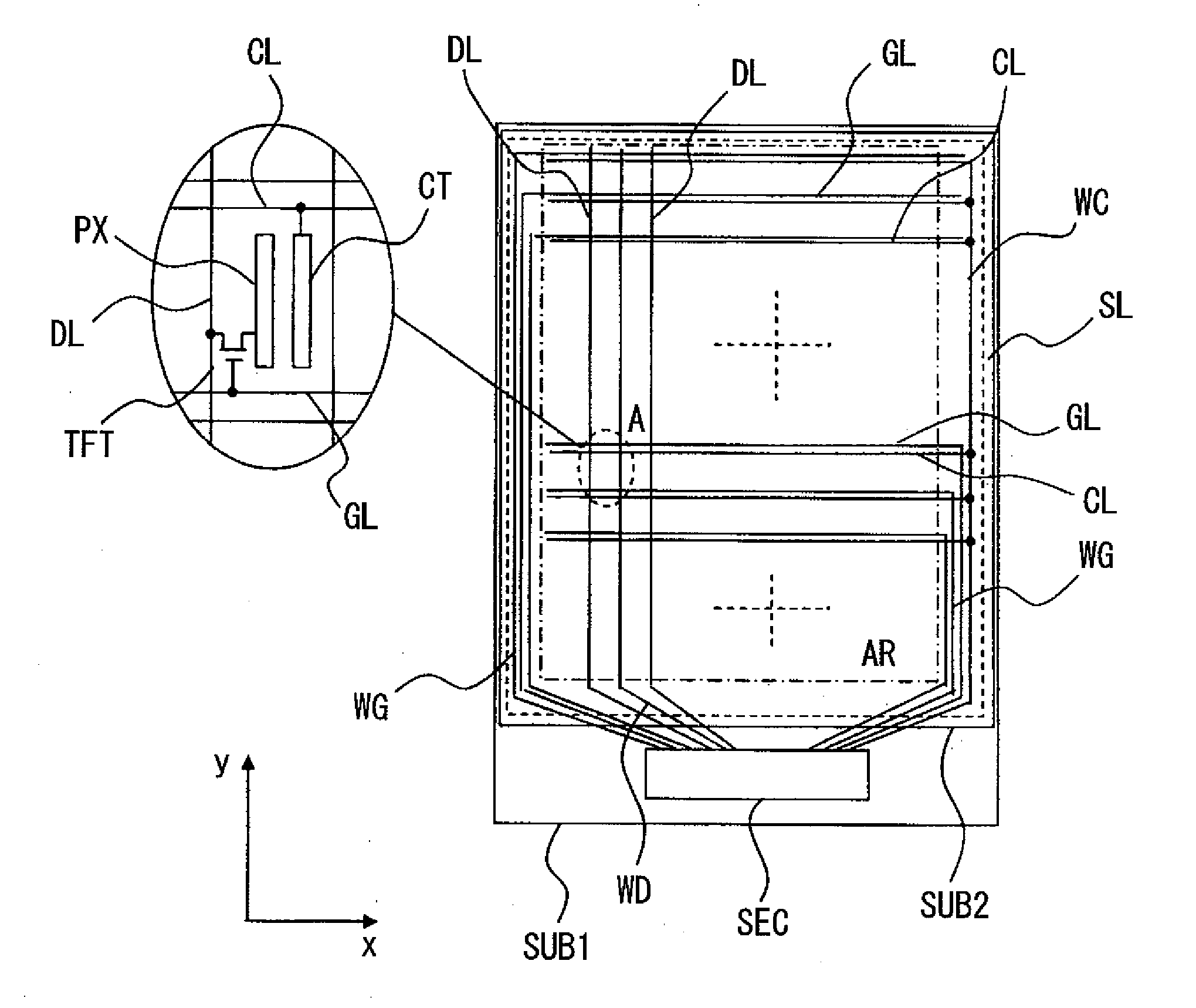
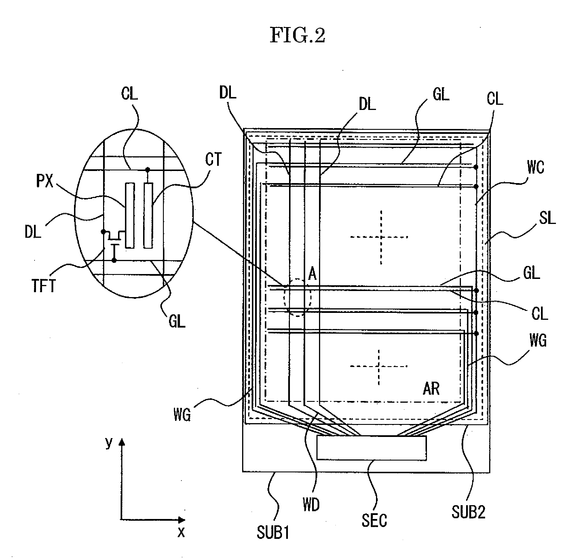
[0061]FIG. 2 is a schematic plan diagram showing the liquid crystal display device according to the first embodiment of the present invention. FIG. 2 shows an example of a liquid crystal display device for a cellular phone, for example.
[0062]In FIG. 2, a substrate SUB1 and a substrate SUB2 are provided so as to face each other and sandwich liquid crystal (not shown) in between. The substrate SUB2 is formed so as to have a slightly smaller area than the substrate SUB1, and positioned so as to expose the lower side portion of the substrate SUB1 as in the figure. A semiconductor device (chip) SEC for driving the pixels in the liquid crystal display device is mounted face down in the side portion on the bottom side of the substrate SUB1 as in the figure.
[0063]An annular sealing material SL is formed around the periphery of the substrate SUB2 between the substrate SUB1 and the substrate SUB2 so that the substrate SUB1 and the substrate SUB2 are pasted together and the above described liq...
second embodiment
[0098]In the first embodiment, the structure of the color filter CF, which also works as a passivation film PAS2, is described as being on the substrate SUB1 side, where thin film transistors TFT are provided. However, the invention is not limited to this, and the present invention may be applied to the color filter CF formed on the substrate SUB2 side where the substrate SUB2 faces the substrate SUB1 having thin film transistors TFT with liquid crystal in between.
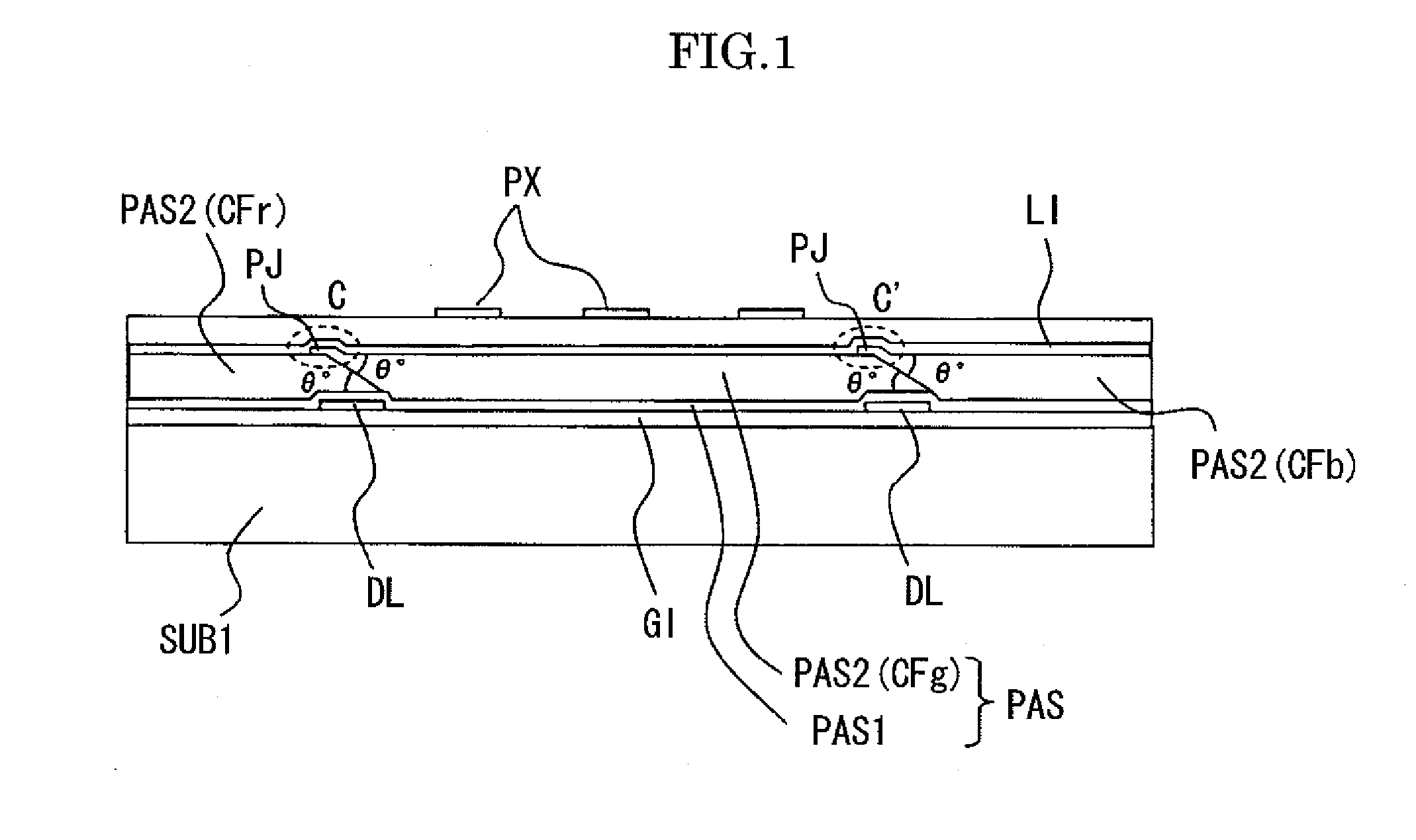
[0099]FIG. 11 is a cross sectional diagram showing a liquid crystal display device formed by applying the present invention. In FIG. 11, a substrate SUB1 and a substrate SUB2 are provided so as to face each other with liquid crystal LC in between. As shown in FIG. 11, which corresponds to FIG. 1, in the structure of the substrate SUB1 on the liquid crystal side, the passivation film PAS2 works only as a passivation film, and not as a color filter. A black matrix (light blocking film) BM which determines the border between ...
third embodiment
[0101]FIG. 12 is a diagram showing the manufacturing method for a liquid crystal display device according to another embodiment of the present invention and corresponds to FIGS. 5A and 5B.
[0102]The structure in FIG. 12 is different from the structure in FIGS. 5A and 5B in the following point. That is to say, two types of protrusions having different heights, which protrude from the light shielding regions SH towards the non-light shielding region NS, are formed along the border between the light shielding regions SH and the light transmitting region NS in the photomask PMr. One type of protrusions D1 has a height of approximately 3.0 μm, and the other type of protrusions D2 has a height of approximately 4.5 μm, for example, and the width of these protrusions is approximately 1.5 μm, and they are aligned alternately with intervals of approximately 1.5 μm, for example. As a result, the border between the light shielding regions SH and the light transmitting region NS has a pattern whe...
PUM
 Abstract
Description
Claims
Application Information
 - R&D Engineer
- R&D Manager
- IP Professional
- Industry Leading Data Capabilities
- Powerful AI technology
- Patent DNA Extraction
Browse by: Latest US Patents, China's latest patents, Technical Efficacy Thesaurus, Application Domain, Technology Topic.
© 2024 PatSnap. All rights reserved.Legal|Privacy policy|Modern Slavery Act Transparency Statement|Sitemap