Reflective mask blank, reflective mask and manufacturing method thereof, and semiconductor device manufacturing method

a reflective mask and masking technology, applied in the field of reflective masking masking and manufacturing methods, can solve the problem of the possibility of the pattern not being drawn as designed, and achieve the effect of fine and highly accurate absorber patterns, reduced film thickness of absorber films, and reduced shadowing effects

Active Publication Date: 2019-12-19
HOYA CORP
View PDF0 Cites 29 Cited by
  • Summary
  • Abstract
  • Description
  • Claims
  • Application Information

AI Technical Summary

Benefits of technology

[0035]According to the reflective mask blank of the present disclosure (and the reflective mask blank produced thereby), the film thickness of an absorber film can be reduced, shadowing effects can be reduced, and a fine and highly accurate absorber pattern can be formed having a stable cross-sectional shape with little sidewall roughness. Thus, a reflective mask produced using a reflective mask blank employing this structure enables the fine and highly accurate formation of a phase shift pattern per se formed on the mask, while also being able to prevent reductions in accuracy during transfer attributable to shadowing. In addition, a method of manufacturing a fine and highly accurate semiconductor device can be provided by carrying out EUV lithography using this reflective mask.

Problems solved by technology

However, since Co and Ni are magnetic, when electron beam drawing is carried out on a resist film on the absorber film deposited using these materials, there is the risk of the possibility of the pattern being unable to be drawn as designed.

Method used


Image

  • Reflective mask blank, reflective mask and manufacturing method thereof, and semiconductor device manufacturing method
  • Reflective mask blank, reflective mask and manufacturing method thereof, and semiconductor device manufacturing method
  • Reflective mask blank, reflective mask and manufacturing method thereof, and semiconductor device manufacturing method

Examples


example 1

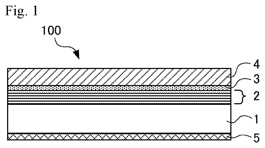
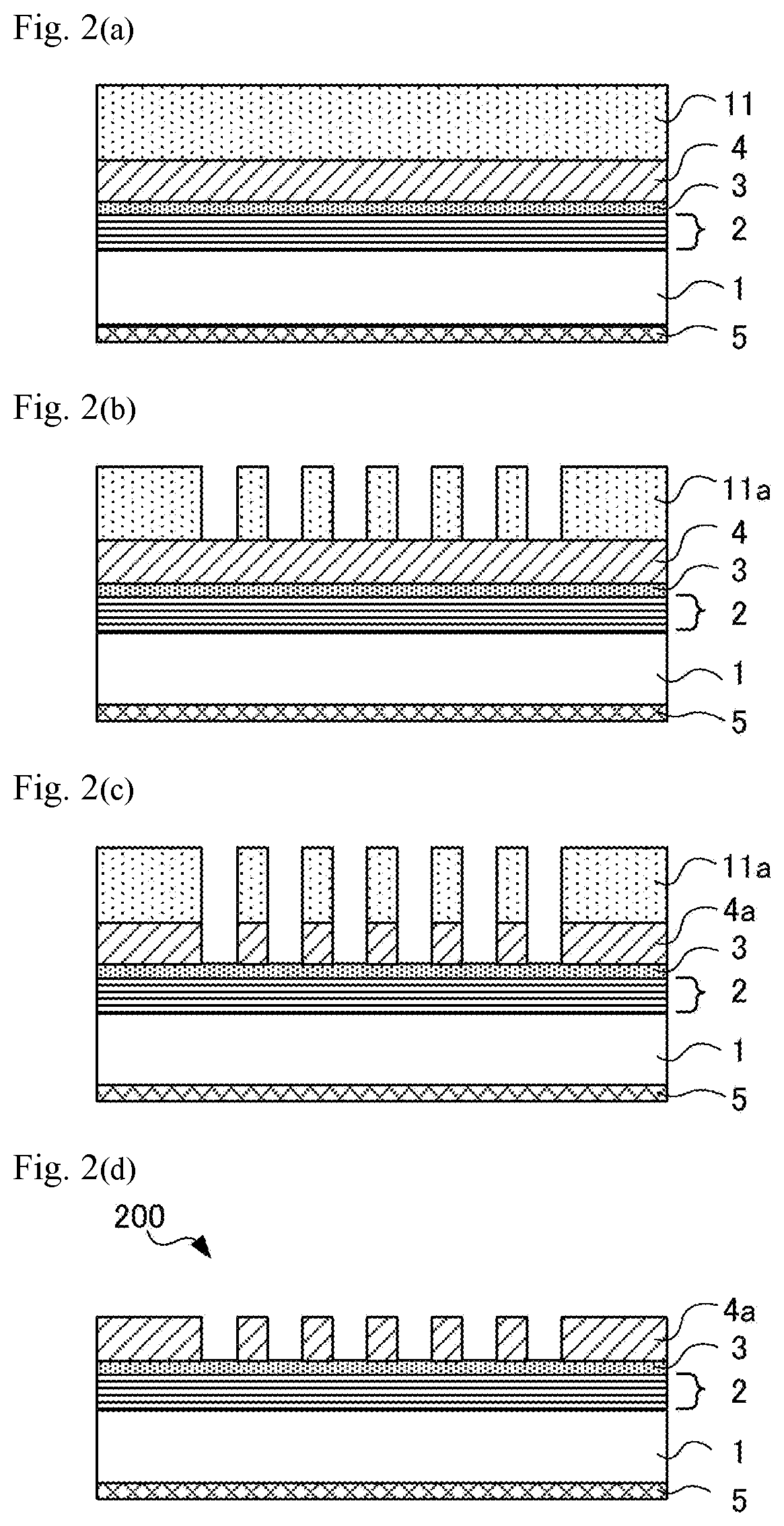
[0145]The reflective mask blank 100 of Example 1 has the back side conductive film 5, the substrate 1, the multilayer reflective film 2, the protective film 3 and the absorber film 4 as shown in FIG. 1. The absorber film 4 is comprised of an amorphous alloy of NiTa. As shown in FIG. 2(a), a resist film 11 is formed on the absorber film 4. FIG. 2 is a cross-sectional schematic diagram of the main portions indicating a process for manufacturing the reflective mask 200 from the reflective mask blank 100.

[0146]First, an explanation is provided of the reflective mask blank 100 of Example 1.

[0147]A 6025 size (approx. 152 mm×152 mm×6.35 mm) low thermal expansion glass substrate in the form of a SiO2-TiO2-based glass substrate, of which both the first main surface and second main surface have been polished, is prepared for use as the substrate 1. Polishing consisting of a coarse polishing step, precision polishing step, local processing step and touch polishing step was carried out so as to...

example 2

[0161]Example 2 is an example of the case of using a NiZr amorphous alloy for the absorber film 4, and is the same as Example 1 with the exception thereof.

[0162]Namely, the absorber film 4 comprised of a NiZr film was formed by DC magnetron sputtering. The NiZr film was deposited at a film thickness of 53.9 nm by reactive sputtering in an Ar gas atmosphere using a NiZr target.

[0163]The element ratio of the NiZr film was 80 at % Ni and 20 at % Zr. In addition, measurement of the crystal structure of the NiZr film by X-ray diffraction (XRD) demonstrated an amorphous structure. In addition, the refractive index n of the NiZr film at a wavelength of 13.5 nm was about 0.952 and the extinction coefficient k was about 0.049.

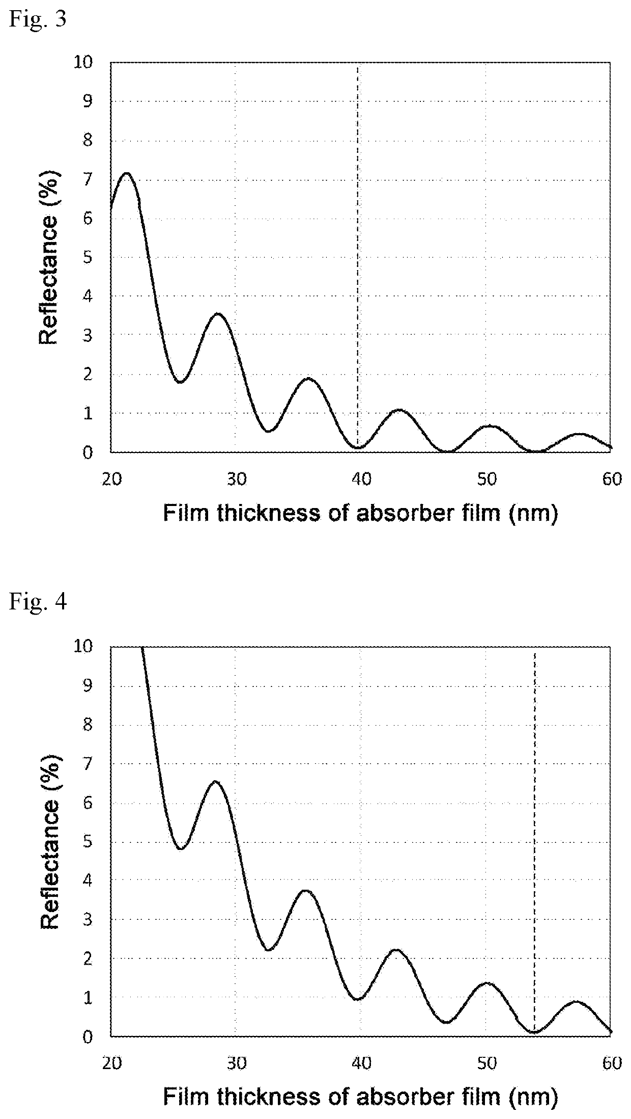
[0164]Reflectance of the absorber film 4 comprised of the aforementioned NiZr film at a wavelength of 13.5 nm was 0.12% since the film thickness was made to be 53.9 nm (FIG. 4).

[0165]In addition, fabrication of the reflective mask 200 and semiconductor device of Example...

example 3

[0166]Example 3 is an example of the case of using a NiP amorphous alloy for the absorber film 4, and is the same as Example 1 with the exception thereof

[0167]Namely, the absorber film 4 comprised of a NiP film was formed by DC magnetron sputtering. The NiP film was deposited at a film thickness of 46.4 nm by reactive sputtering in an Ar gas atmosphere using a NiP target.

[0168]The element ratio of the NiP film was 79.5 at % Ni and 20.5 at % P. In addition, measurement of the crystal structure of the NiP film by X-ray diffraction (XRD) demonstrated an amorphous structure. In addition, the refractive index n of the NiP film at a wavelength of 13.5 nm was about 0.956 and the extinction coefficient k was about 0.056.

[0169]Reflectance of the absorber film 4 comprised of the aforementioned NiP film at a wavelength of 13.5 nm was 0.13% since the film thickness was made to be 46.4 nm (FIG. 5).

[0170]In addition, fabrication of the reflective mask 200 and semiconductor device of Example 3 in ...


PUM

PropertyMeasurementUnit
wavelengthaaaaaaaaaa

Abstract

Provided are a reflective mask blank and a reflective mask, which are able to reduce the shadowing effects of EUV lithography and form a fine pattern. As a result, a semiconductor device can be stably manufactured with high transfer accuracy. The reflective mask blank comprises a multilayer reflective film and an absorber film in that order on a substrate, and the absorber film comprises a material comprising an amorphous metal comprising at least one or more elements among cobalt (Co) and nickel (Ni).

Description

CROSS REFERENCE TO RELATED APPLICATIONS[0001]This application is the U.S. National Phase application of International Application No. PCT / JP2018 / 007897, filed Mar. 1, 2018, which claims priority to Japanese Application No. 2017-039100, filed Mar. 2, 2017, and the contents of which is hereby incorporated by reference herein in its entirety.TECHNICAL FIELD[0002]The present disclosure relates to a production master for manufacturing an exposure mask used in the manufacturing of semiconductor devices and the like in the form of a reflective mask blank, a reflective mask, a production method thereof and a method of manufacturing a semiconductor device.BACKGROUND ART[0003]The types of light sources of exposure apparatuses used in the production of semiconductor devices are evolving while gradually using shorter wavelengths, as is indicated by the g-line having a wavelength of 436 nm, i-line having a wavelength of 365 nm, KrF lasers having a wavelength of 248 nm and ArF lasers having a wav...

Claims


Application Information

Patent Timeline
Patent Type & Authority Applications(United States)
IPC IPC(8): G03F1/24G03F1/52G03F1/54
CPCG03F1/52G03F1/54G03F7/2004H01L21/0274G03F1/24G03F1/22G03F1/80G03F7/70033H01L21/027H01L21/31144
Inventor IKEBE, YOHEIHORIKAWA, JUNICHIONOUE, TAKAHIROKATAOKA, MIZUKI
Owner HOYA CORP
Why Eureka
Try Eureka