Reflective mask blank, reflective mask and method for manufacturing same, and method for manufacturing semiconductor device

a technology of reflective masks and masks, applied in the field of reflective masks and methods for manufacturing same, can solve problems such as shadowing effects

Pending Publication Date: 2021-10-07
HOYA CORP
View PDF8 Cites 0 Cited by
  • Summary
  • Abstract
  • Description
  • Claims
  • Application Information

AI Technical Summary

Problems solved by technology

Since in EUV lithography, the exposure light is obliquely incident with respect to the reflective mask, there is an inherent problem called a shadowing effect.

Method used


Image

  • Reflective mask blank, reflective mask and method for manufacturing same, and method for manufacturing semiconductor device
  • Reflective mask blank, reflective mask and method for manufacturing same, and method for manufacturing semiconductor device
  • Reflective mask blank, reflective mask and method for manufacturing same, and method for manufacturing semiconductor device

Examples


examples

[0170]Hereinafter, Examples will be described with reference to the drawings. The present disclosure is not limited to these Examples.

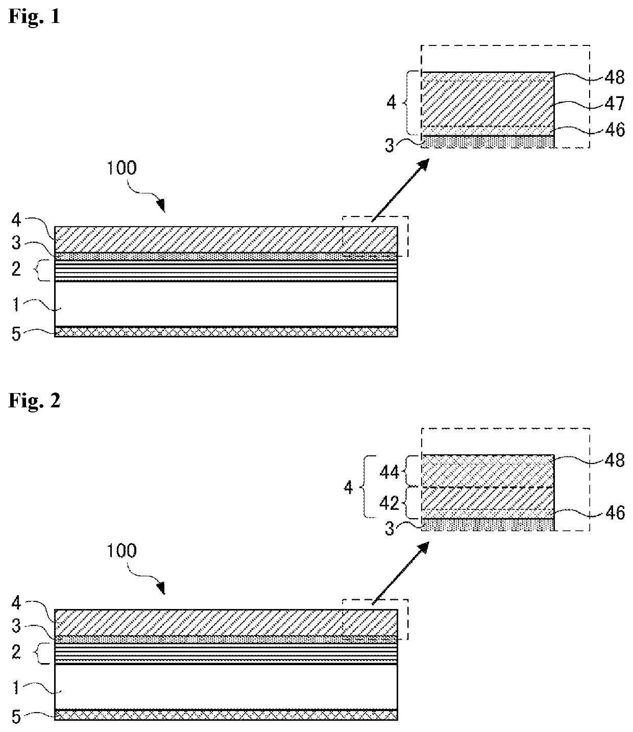
[0171]FIG. 1 shows a structure of reflective mask blanks 100 of Examples 1 to 15. The reflective mask blanks 100 of the Examples each include a conductive back film 5, a substrate 1, a multilayer reflective film 2, a protective film 3, and an absorber film 4. Table 1 shows materials and film thicknesses of the absorber films 4 of the reflective mask blanks 100 of the Examples. As shown in Table 1, the absorber films 4 of Examples 1 to 15 each include two layers, that is, a lower layer 42 and an upper layer 44. Note that the reflective mask blanks 100 of Reference Examples 1 and 2 were manufactured as objects for comparison to the Examples. As shown in Table 1, the absorber films 4 of Reference Examples 1 and 2 each include only a single layer (upper layer 44).

[0172]The reflective mask blank 100 of the Examples and Reference Examples will be specifical...


PUM

PropertyMeasurementUnit
wavelengthaaaaaaaaaa

Abstract

Provided is a reflective mask blank that can reduce the shadowing effect of a reflective mask and form a fine and high-precision absorbent body pattern.
The reflective mask blank comprises a substrate, a multi-layer reflective film disposed on the substrate, and an absorbent body film disposed on the multi-layer reflective film, and is characterized in that: the absorbent body film includes, in at least a part thereof, at least one element with a high absorption coefficient, chosen from the group consisting of cobalt (Co) and nickel (Ni), and an element that increases the speed of dry etching; the absorbent body film includes a lower-surface region that includes a surface on the substrate side and an upper-surface region that includes a surface on the side opposite the substrate; and the concentration (atomic percentage) of the element with the high absorption coefficient in the upper-surface region is greater than the concentration (atomic percentage) of the element with the high absorption coefficient in the lower-surface region.

Description

CROSS-REFERENCE TO RELATED APPLICATIONS[0001]This application is a National Stage of International Application No. PCT / JP2019 / 031361, filed Aug. 8, 2019, which claims priority to Japanese Patent Application No. 2018-159970, filed Aug. 29, 2018, and the contents of which are incorporated by reference.TECHNICAL FIELD[0002]The present disclosure relates to a reflective mask used for manufacturing a semiconductor device and the like, and a reflective mask blank used for manufacturing the reflective mask. The present disclosure also relates to a method of manufacturing a semiconductor device using the above reflective mask.BACKGROUND ART[0003]The wavelengths of light sources of exposure apparatuses in manufacturing semiconductor devices have been gradually shortened. Specifically, the wavelength of the light source has been gradually shortened to 436 nm (g line), 365 nm (i line), 248 nm (KrF laser), and 193 nm (ArF laser). In order to achieve further finer pattern transfer, extreme ultra...

Claims


Application Information

Patent Timeline
Patent Type & Authority Applications(United States)
IPC IPC(8): G03F1/24G03F1/54
CPCG03F1/24G03F1/54
Inventor KATAOKA, MIZUKIIKEBE, YOHEI
Owner HOYA CORP
Why Eureka
Try Eureka