Method of fabricating nanosized filamentary carbon devices over a relatively large-area

Active Publication Date: 2010-10-21
STMICROELECTRONICS SRL
View PDF3 Cites 0 Cited by
  • Summary
  • Abstract
  • Description
  • Claims
  • Application Information

AI Technical Summary

Benefits of technology

[0018]The fact that the electric field orienting bias during the growth process of the CNTs is self-generated by the contact potential difference makes the process of oriented growth self-stopping on acc

Problems solved by technology

The technique suffers in that the heavy top electrode may distort the growing CNTs and is scarcely equipped to determine, a priori, the exact lengths of the grown CNTs when fabricating multiple

Method used


Image

  • Method of fabricating nanosized filamentary carbon devices over a relatively large-area
  • Method of fabricating nanosized filamentary carbon devices over a relatively large-area
  • Method of fabricating nanosized filamentary carbon devices over a relatively large-area

Examples


Embodiment Construction

[0022]The following description made with direct reference to the attached drawings is intended only for illustrative, not limiting, purposes and reports only exemplary embodiments, and, when so-stated, certain preferred choices of materials, techniques and conditions used. The invention may be practiced in many alternative ways to the exemplarily detailed ones, as will immediately appear to the skilled reader.

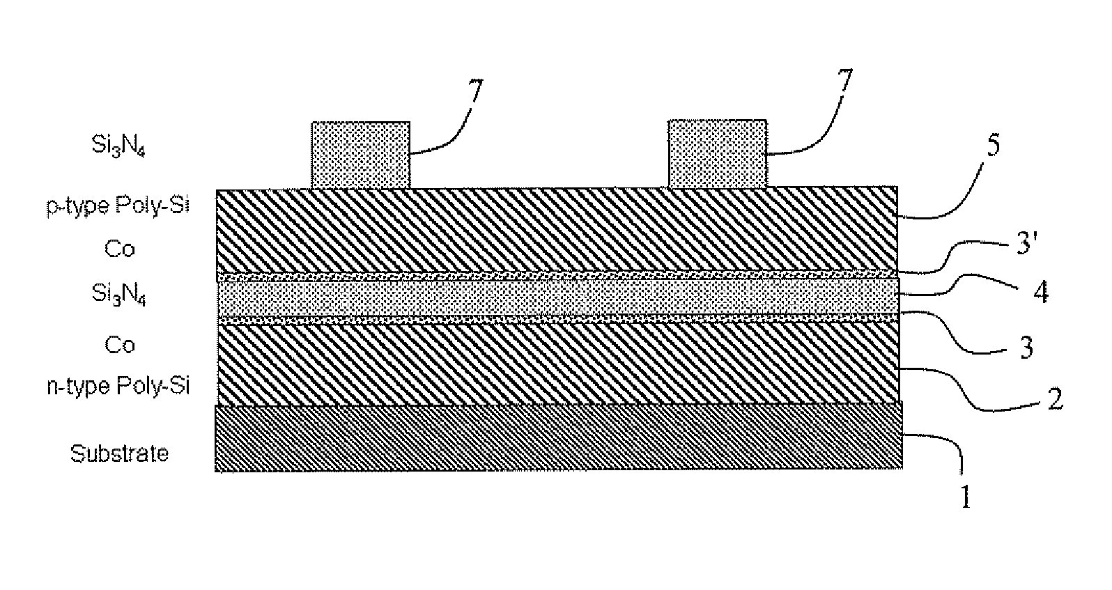
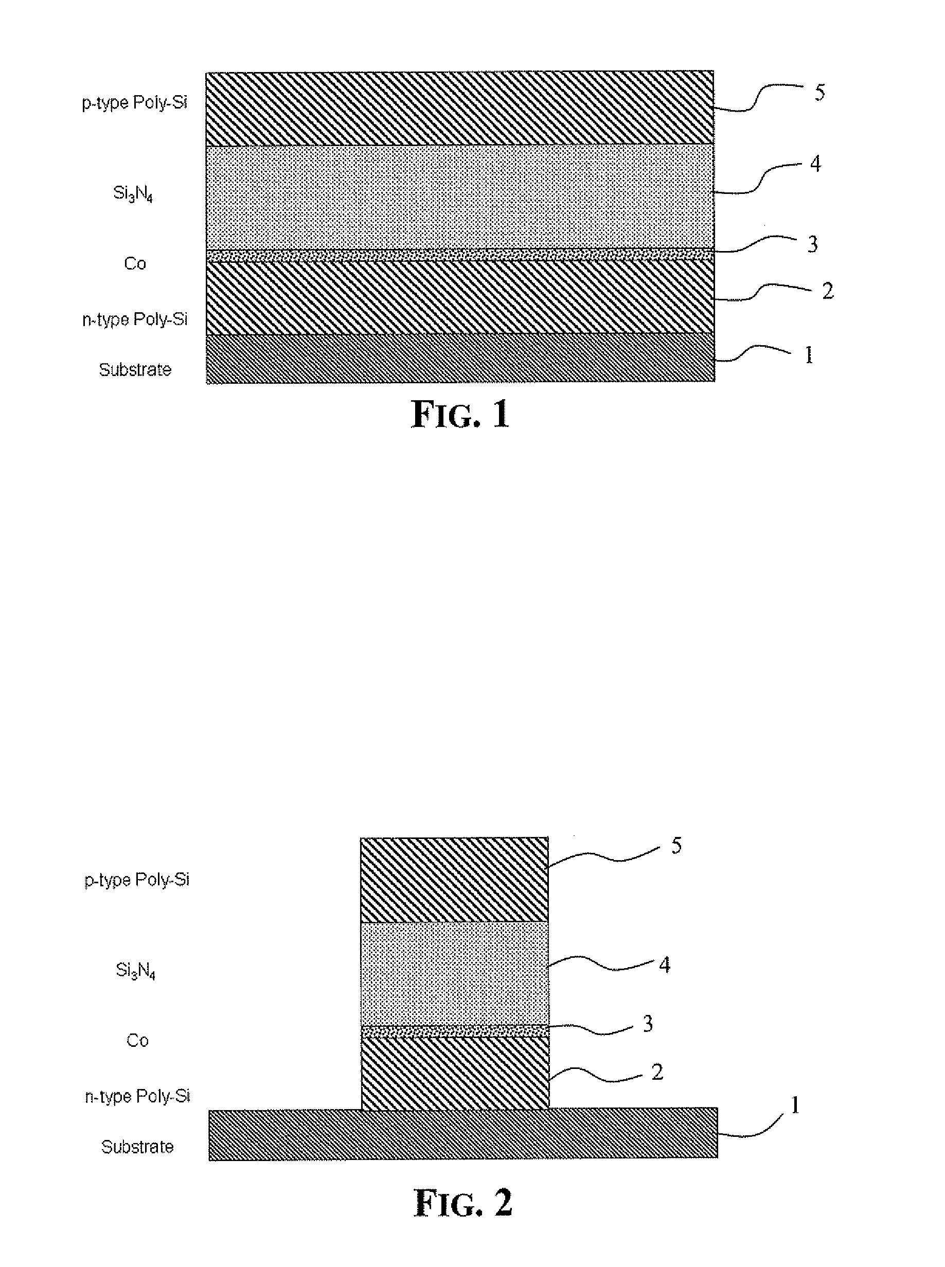
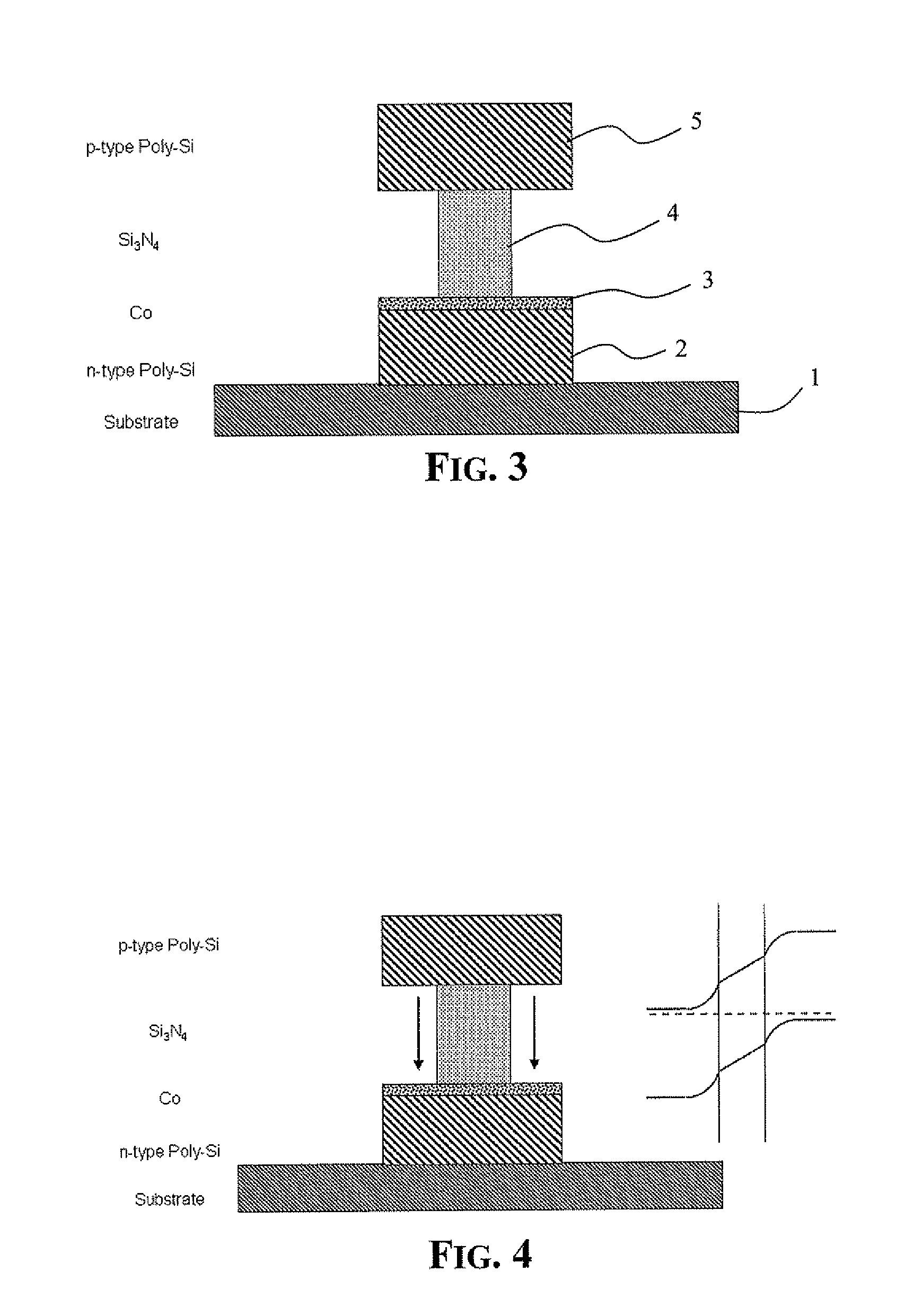
[0023]FIG. 1 schematically illustrates a basic multilayer stack that may be preliminarily formed for eventually forming a CNT in lithographically definable parts of the so-patterned stack. Although in many specific embodiments of the method, a substrate may not be required. In the exemplary general illustration of FIG. 1, a solid substrate 1 is shown having a generally flat surface. The optional substrate 1 may be of one of innumerable suitable materials such as monocrystalline silicon, polycrystalline silicon, silica, alumina, porous monocrystalline silicon, zeolite sapphire,...


PUM


Abstract

Nanosized filamentary carbon structures (CNTs) nucleating over a catalyzed surface may be grown in an up-right direction reaching a second surface, spaced from the first surface, without the need of applying any external voltage source bias. The growth process may be inherently self-stopping, upon reaching a significant population of grown CNTs on the second surface. A gap between the two surfaces may be defined for CNT devices being simultaneously fabricated by common integrated circuit integration techniques. The process includes finding that for separation gaps of up to a hundred or more nanometers, a difference between the respective work functions of the materials delimiting the gap space, for example, different metallic materials or a doped semiconductor of different dopant concentration or type, may produce an electric field intensity orienting the growth of nucleated CNTs from the surface of one of the materials toward the surface of the other material.

Description

FIELD OF THE INVENTION[0001]The present disclosure relates in general to nanosized filamentary carbon structures, typically carbon nanotubes (mono or multi walled) and / or carbon nanowires, (CNTs), and related functional devices. In particular, to a method of growing oriented nanosized filamentary carbon structures, typically carbon nanotubes (mono or multi walled) and / or carbon nanowires (CNTs) over defined areas of a relatively large substrate with techniques that are commonly practiced in the semiconductor manufacturing industry to enable integration of active or passive CNT parts in electronic devices.BACKGROUND OF THE INVENTION[0002]The mainstream of semiconductor industry progress is primarily driven by the ability of shrinking the size of basic structures of an integrated circuit (IC), for example, the metal oxide semiconductor field effect transistor (MOSFET). New materials of peculiar electrical and physical characteristics, in addition to the traditional materials of microe...

Claims


Application Information

Patent Timeline
IPC IPC(8): H01L29/66H01L21/20
CPCB82Y10/00H01L51/0012H01L51/057H01L51/05H01L51/0048Y10S977/89Y10S977/742Y10S977/901H10K71/191H10K85/221H10K10/00H10K10/491
Inventor MASCOLO, DANILOBEVILACQUA, MARIA FORTUNA
Owner STMICROELECTRONICS SRL
Why Eureka
Try Eureka