Field plate trench mosfet transistor with graded dielectric liner thickness

a dielectric liner and trench mosfet technology, applied in the field of semiconductor devices, can solve the problems of power dissipation and/or low area consumption during mosfet operation

Inactive Publication Date: 2010-10-21
TEXAS INSTR INC
View PDF22 Cites 66 Cited by
  • Summary
  • Abstract
  • Description
  • Claims
  • Application Information

AI Technical Summary

Benefits of technology

[0006]In accordance with the standard practice in the semiconductor industry, various features of the accompanying drawings may not be drawn to scale. In fact, the dimensions of the various features may be arbitrarily increased or reduced for clarity of discussion. Furthermore, in certain embodiments, reference may be made to vertical or horizontal directions. No

Problems solved by technology

A lower specific on-resistance results in lower area consump

Method used


Image

  • Field plate trench mosfet transistor with graded dielectric liner thickness
  • Field plate trench mosfet transistor with graded dielectric liner thickness
  • Field plate trench mosfet transistor with graded dielectric liner thickness

Examples


Embodiment Construction

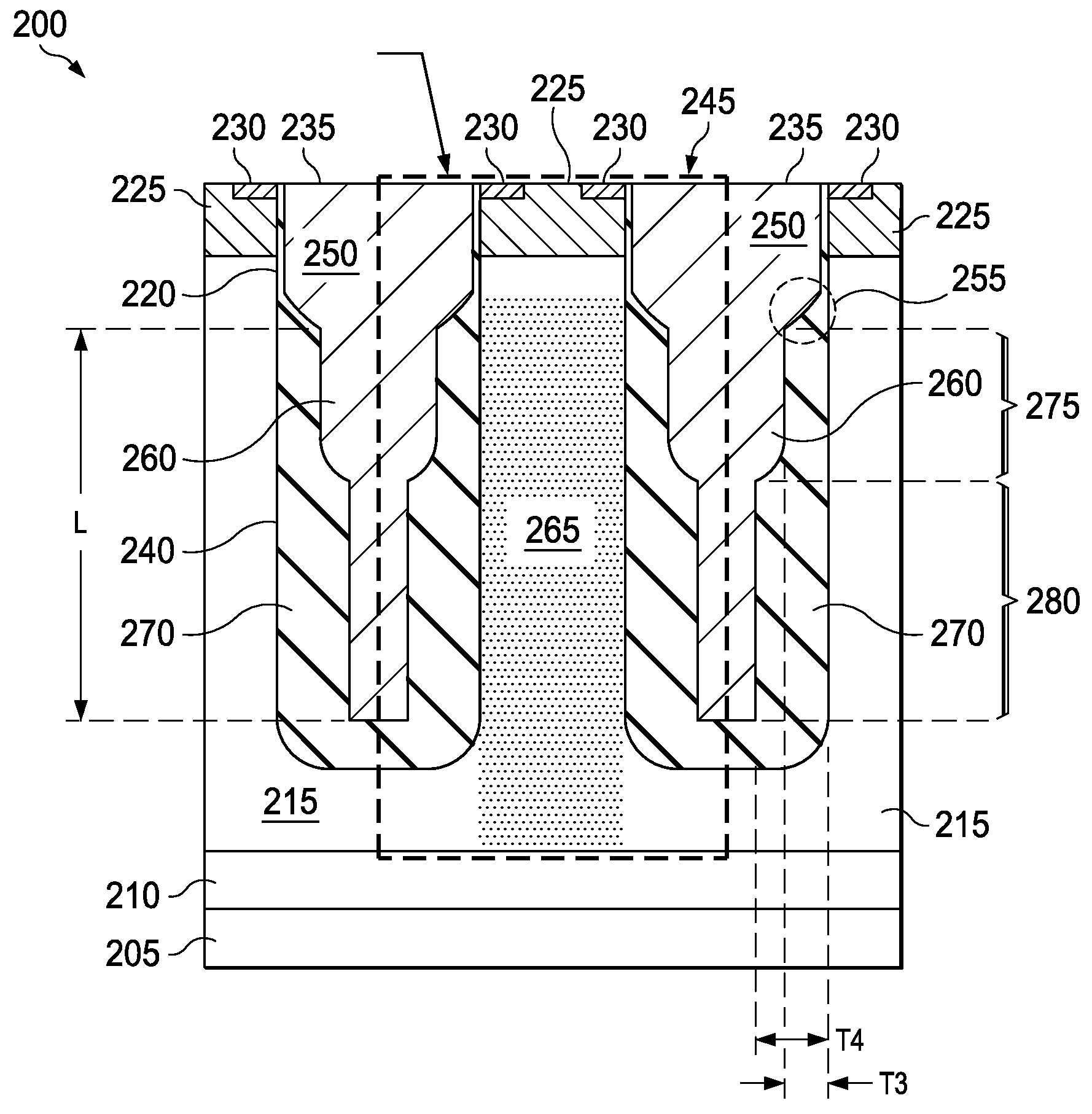
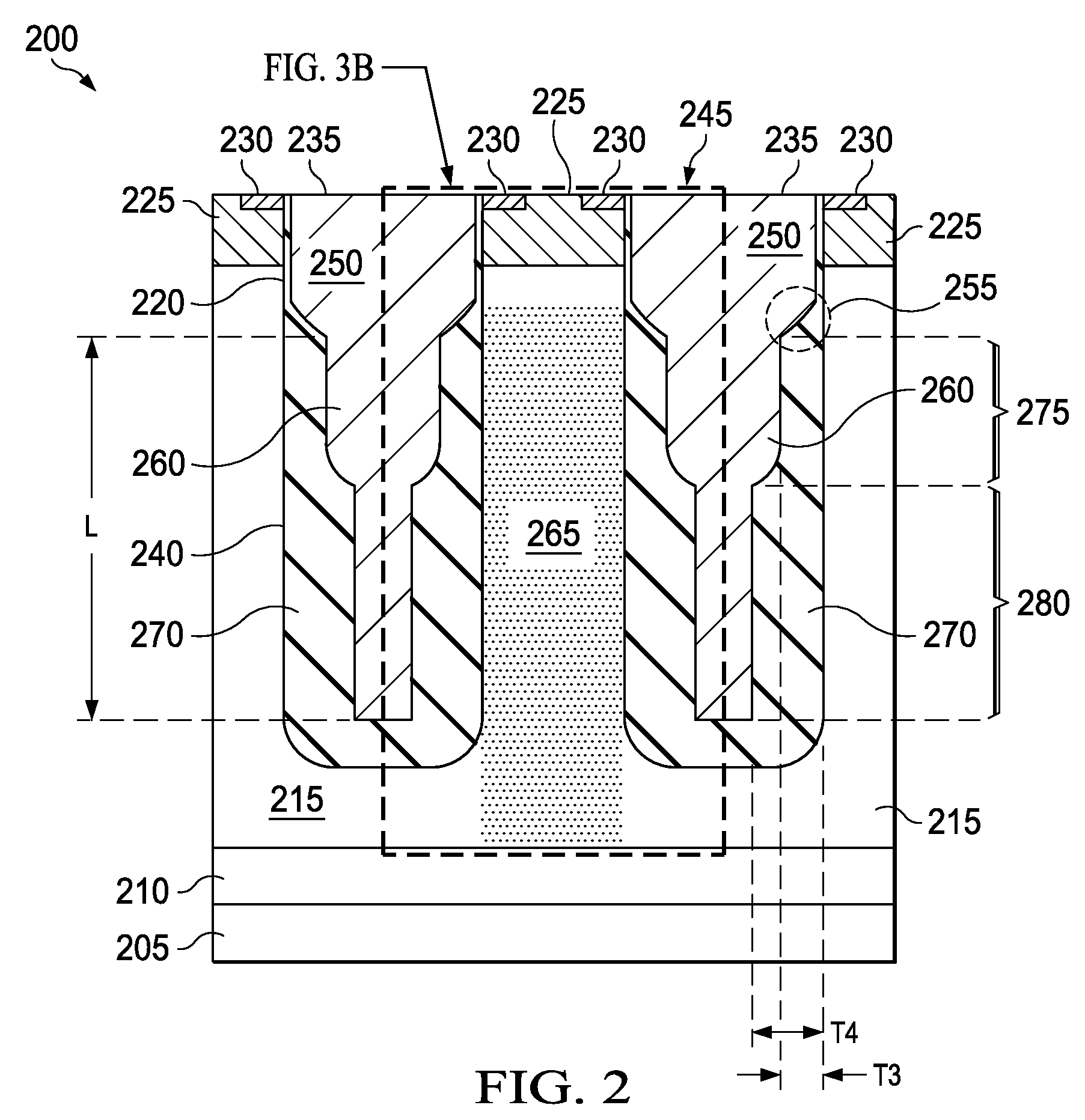
[0011]A trench field plate MOSFET includes a number of field plates formed within a drain extension region. The disclosure benefits from the recognition that operating characteristics of a trench field plate MOSFET may be improved by providing a dielectric between the field plates and the drain extension region that has a variable thickness therebetween. The variable thickness is expected to provide a flatter potential distribution in the direction of carrier flow during operation, resulting in increased blocking voltage, e.g.

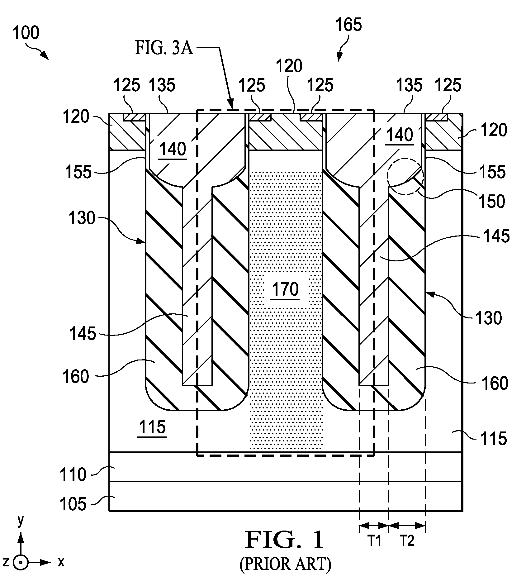
[0012]FIG. 1 illustrates a portion of a prior art trench field plate power MOSFET 100 (hereinafter referred to as the MOSFET 100). Coordinate axes are shown for reference. The illustrated portion includes a substrate 105 with a drain 110 and a drain extension 115 located thereover. A body 120 (sometimes referred to as a backgate) is located over the extension 115, with a source 125 formed over the body 120. The drain 110, the extension 115 and the source 125 ma...


PUM


Abstract

An electronic device has a plurality of trenches formed in a semiconducting layer. A vertical drift region is located between and adjacent the trenches. An electrode is located within each trench, the electrode having a gate electrode section and a field plate section. A graded field plate dielectric is located between the field plate section and the vertical drift region.

Description

TECHNICAL FIELD[0001]This application is directed, in general, to a semiconductor device and, more specifically, to an electronic device employing a vertical drift region.BACKGROUND[0002]Trench field plate MOSFET transistors provide a vertical drift region architecture to reduce the area of the transistor. A general objective of MOSFET design is to minimize the specific on-resistance, Rsp, of the transistor, e.g., the product of the device area A and its on-state resistance Ron. A lower specific on-resistance results in lower area consumption and / or power dissipation during operation of the MOSFET.SUMMARY[0003]One aspect provides an electronic device that has a plurality of trenches formed in a semiconducting layer. A vertical drift region is located between and adjacent the trenches. An electrode is located within each trench, the trench having a gate electrode section and a field plate section. A graded field plate dielectric is located between the field plate section and the vert...

Claims


Application Information

Patent Timeline
IPC IPC(8): H01L29/78H01L21/28H01L21/336
CPCH01L29/42368H01L29/7813H01L29/66734H01L29/66719H01L29/407H01L29/41
Inventor DENISON, MARIEPENDHARKAR, SAMEERHOWER, PHILIP L.LIN, JOHN
Owner TEXAS INSTR INC
Why Eureka
Try Eureka