Supercharge Your Innovation With Domain-Expert AI Agents!

Image processing circuit and image processing method thereof

Inactive Publication Date: 2010-11-18
NOVATEK MICROELECTRONICS CORP
View PDF10 Cites 4 Cited by
  • Summary
  • Abstract
  • Description
  • Claims
  • Application Information

AI Technical Summary

Benefits of technology

[0014]Accordingly, the present invention is directed to an image processing method, which is able to produce a corresponding weight value according to the pixel difference value of each pixel of an input video signal, judge the area where the pixels are located in and further perform corresponding low-pass filtering processing, peaking processing or luminance transient improvement processing (LTI processing) on the pixels. By using the image processing method, the light contours or dark contours of the frames are avoided after the sharpening processing.
[0015]The present invention is also directed to an image processing circuit, which is able to produce a corresponding weight value according to the pixel difference value of each pixel of an input video signal, judge the area where the pixels are located in and further perform corresponding low-pass filtering processing, peaking processing or LTI processing on the pixels according to the different areas where the pixels are located in. In this way, high-quality frames are obtained.
[0036]Based on the description above, the present invention is able to select an appropriate processing to process each pixel of the input video signal according to the pixel difference value of the pixel, wherein the processing includes low-pass filtering processing, peaking processing, and LTI processing. On pixels with lower pixel difference values, the low-pass filtering processing is performed so that the corresponding area within a frame look more smooth; on pixels with higher pixel difference values, the LTI processing is performed so that no light contours and dark contours appear in the corresponding area within a frame. On pixels with moderate pixel difference values, the peaking processing is performed so that the profiles and the edges of the image objects in the corresponding area within a frame are more clear. In addition, the corresponding weight values of a sharpening processing are adaptively defined according to different pixel difference values, so that the frame after the sharpening processing looks more clear and natural.

Problems solved by technology

Although the sharpening processing can gain a higher contrast of the profiles or the edges of the image objects, but it may cause negative effect as well.
For an image where the edges of the objects are clear already, a further sharpening processing may make the edges thereof generate unacceptable visual effect such as light contour.

Method used


Image

  • Image processing circuit and image processing method thereof
  • Image processing circuit and image processing method thereof
  • Image processing circuit and image processing method thereof

Examples


Embodiment Construction

[0053]Reference will now be made in detail to the present preferred embodiments of the invention, examples of which are illustrated in the accompanying drawings. Wherever possible, the same reference numbers are used in the drawings and the description to refer to the same or like parts.

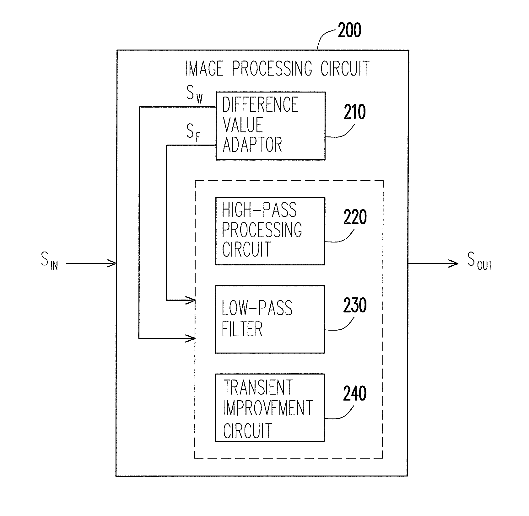
[0054]FIG. 5 is a function block diagram of an image processing circuit 200 according to an embodiment of the present invention. Referring to FIG. 5, the image processing circuit 200 receives and processes an input video signal SIN so as to produce an output video signal SOUT. The input video signal SIN carries the information of pixel values of a plurality of pixels used for a display to display a corresponding frame. The pixel values carried by the input video signal SIN are sequentially input to the image processing circuit 200. FIG. 6 is a diagram showing partial pixels of an input video signal SIN according to an embodiment of the present invention. Referring to FIG. 6, the pixel values of a plu...


PUM


Abstract

An image processing circuit and an image processing method thereof are disclosed. A difference value adaptor of the image processing circuit produces a weighing value and a flag value corresponding to the pixel according to the pixel difference value of each pixel of an input video signal. The image processing circuit judges which area among a first area, a second area and a third area the pixel difference value of each pixel falls in according to the flag value. The image processing circuit performs a low-pass filtering processing on the pixel having the pixel difference value falling in the first area, performs a high-pass filtering processing on the pixel having the pixel difference value falling in the second area and performs a luminance transient improvement processing (LTI processing) on the pixel having the pixel difference value falling in the third area.

Description

CROSS-REFERENCE TO RELATED APPLICATION[0001]This application claims the priority benefit of Taiwan application serial no. 98116402, filed on May 18, 2009. The entirety of the above-mentioned patent application is hereby incorporated by reference herein and made a part of specification.BACKGROUND OF THE INVENTION[0002]1. Field of the Invention[0003]The present invention generally relates to an image processing circuit and an image processing method thereof, and more particularly, to an image processing circuit and an image processing method thereof for performing adaptive processing according to the image characteristic.[0004]2. Description of Related Art[0005]When watching images, a viewer pays attention to not only the color and the hue of the images, but also to the profiles or the edges of the objects in the images. The image processing is used to enhance the image features for improving or increasing the visual effect of the images. For example, images obtained by a digital came...

Claims


Application Information

Patent Timeline
IPC IPC(8): H04N5/217
CPCG06T5/003G06T5/20H04N5/142G06T2207/20012G06T2207/10016G06T5/73
Inventor CHEN, WEI-FUKUO, CHIH-CHIA
Owner NOVATEK MICROELECTRONICS CORP
Features
  • R&D
  • Intellectual Property
  • Life Sciences
  • Materials
  • Tech Scout
  • Unparalleled Data Quality
  • Higher Quality Content
  • 60% Fewer Hallucinations
Learn More